标签:des style blog http color os
Embodiments of the invention describe a dynamic random access memory (DRAM) device that may abort a self-refresh mode to improve the exit time from a DRAM low power state of self-refresh. During execution of a self-refresh mode, the DRAM device may receive a signal (e.g., a device enable signal) from a memory controller operatively coupled to the DRAM device. The DRAM device may abort the self-refresh mode in response to receiving the signal from the memory controller.
Embodiments of the invention generally pertain to electronic devices, and more particularly to systems, apparatuses and methods to improve the exit time from a dynamic random access memory (DRAM) low power state of self-refresh.
Memory cells in a DRAM device include a transistor and a capacitor to store a bit of data. The memory cells are ‘dynamic‘ because their data decays and becomes invalid due to various leakage current paths to surrounding cells and to the substrate of the device. To keep the data in the cells valid, each memory cell is periodically refreshed.
Every row of cells in a DRAM memory array needs to be refreshed before the data in the row decays to an invalid state. There are two types of refreshes: external refreshes and internal refreshes (i.e., the DRAM device places itself in self-refresh mode).
During internal DRAM memory refreshes, the memory controller has no visibility to when this refresh is initiated. As a result, the controller is designed to wait for an entire refresh cycle (tRFC, plus a guard band, e.g., 10 ns) before issuing a command to the DRAM. The time period a memory controller must wait before issuing a valid command is herein referred to as tXS (i.e., tRFC+10 ns). tRFC for a 2 Gbit device is in the range of 160 ns. The tRFC approximately doubles as DRAM devices increase in density (e.g., tRFC for a 4 GBit device is in the range of 300 ns, tRFC for an 8 Gbit device is in the range of 550 ns), thus increasing tXS.
Therefore it is desirable to reduce the value of tXS for DRAM devices in order to reduce the time a memory controller must wait before issuing valid commands.
Embodiments of the invention describe a DRAM device that may abort a self-refresh mode to improve the exit time from a DRAM low power state of self-refresh. A self-refresh mode is to be understood as a mode to refresh rows of a DRAM device. This mode is managed internally by the DRAM—the DRAM controller has no visibility to when the refresh mode is initiated.
In the prior art, the DRAM controller is designed to wait for a refresh cycle (tRFC) to complete (tRFC plus and a guard band value, e.g. 10 ns) before issuing a command to the DRAM. By enabling a DRAM device to abort a self-refresh mode, the DRAM controller has a significantly shorter wait period before it may issue a command to the DRAM. In one embodiment, a DRAM device is enabled by the memory controller to abort self-refresh modes in order to maintain the option of the DRAM device functioning according to the prior art (i.e., execute a full self-refresh cycle).
FIG. 1?is a block diagram of selected components of a computing system utilizing an embodiment of the invention. Computing system?100?includes a plurality of processors (e.g., central processing units and/or cores)?150-1through?150-n, memory controller?110, memory?115?including (at least one) DRAM memory device?130, and interconnect?120. Memory controller?110controls, at least in part, the transfer of information between system components and memory?115, and thus the transfer of information between system components and DRAM memory?130. Said system components may include processors?150-1?through?150-n, an input/output device (e.g., a peripheral component interconnect (PCI) Express device), memory itself, or any other system component that requests access to memory?115. In other embodiments, memory controller?110?may be included (or integrated) with a system processor.
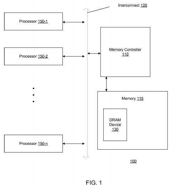
Both memory controller?110?and DRAM device?130?may cause a refresh of the DRAM memory cells to occur. Memory controller?110?may issue a command to DRAM device?130?to refresh some or all of its memory cells. DRAM device?130?may also execute a "self-refresh" mode—essentially a plurality of commands to refresh the cells of the device (e.g., each command may execute a refresh of a plurality of rows).
In this embodiment, memory controller?110?is responsible for "enabling" DRAM?130?(e.g., asserting a "clock enable" signal). DRAM?130?may abort an executing self-refresh mode in response to receiving the enable signal from memory controller?110(or a dedicated signal from memory controller?110?initialing the exit from self-refresh mode). It is to be understood that aborting an executing self-refresh mode allows for a significant reduction in the time memory controller?110?must wait before issuing a valid command (i.e., tXS). Thus, aborting a self-refresh mode is also referred to herein as a fast exit from DRAM self refresh. Operations describing how DRAM?130?may abort said self-refresh mode are described below.
DRAM device?130?may require memory controller?110?to "enable" the device to abort self-refresh modes (i.e., enable "fast exit" mode for the device). If the "fast exit" mode is not enabled, then DRAM device?130?will not abort the self-refresh mode. Memory controller?110?will be aware if "fast exit" mode is or is not enabled, and adjust the timing of issuing commands to the DRAM device accordingly.
FIG. 2?is a block diagram of components of a DRAM device utilizing an embodiment of the invention. In this example, a DRAM memory includes (at least one) double-data rate (DDR) 4×4 device?200. DRAM device?200?may include plurality of memory banks?201-216?(other embodiments may be utilized by devices including more or less banks). Memory banks?201-216?may have differing types of memory cells in some embodiments (e.g., one type of memory cell may be faster than others or may consume more or less power compared with other memory cell types). Moreover, various types of DRAM may be utilized for the memory banks shown in?FIG. 2, including for example, Graphics DRAM, Fast DRAM, Low Power DRAM, etc.
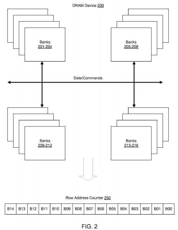
Banks?201-216?may be organized within four bank groups, each group including four banks (i.e., group?201-204,?205-208,209-212?and?213-216). In this example, 32 bits of data are transferred for every read or write access.
According to the DDR3 specification (as defined by JEDEC JESD79-3) the refresh period is 64 ms and refresh interval is 7.8 us. This translates to 8K refresh commands during the refresh period (64 ms/7.8 us=8K). In this example, DRAM device200?has 32K rows per bank; thus each refresh command will refresh four rows of memory (32K/8K=4).
A self-refresh mode executed by DRAM device?200?may be aborted during the execution of a refresh command (i.e., during the refresh of four rows of memory in this embodiment). It is to be understood that when DRAM device?200?receives an indication to abort a self-refresh mode (e.g., a device enable signal from the DRAM controller, a dedicated signal from the controller to abort the self-refresh, etc.), it may increase the efficiency of subsequent self-refresh mode executions to keep track of which rows were able to be refreshed, and which rows have yet to be refreshed. Row refreshes may be kept track of through row address counter?250?containing bits B14-B0—because there are 32 k rows per bank, DRAM device?200would require 15 row address bits for row address counter?250.
Because four rows of memory are refreshed per refresh command in this embodiment, two bits (e.g., B0?and B1) may indicate the specific row to refresh, and the remaining bits indicate which bank group and bank includes the row to be refreshed. In this example, at the start of each refresh command, bits B1?and B0?are 00. If a refresh command is issued then the remaining row address bit segment (e.g., B14-B2) is incremented by one and bits B1?and B0?cycle thru 00, 01, 10 and 11. This assumes that four rows of memory are refreshed in all the banks.
FIG. 3?is a flow diagram of an embodiment of the invention. Flow diagrams as illustrated herein provide examples of sequences of various process actions. Although shown in a particular sequence or order, unless otherwise specified, the order of the actions can be modified. Thus, the illustrated implementations should be understood only as examples, and the illustrated processes can be performed in a different order, and some actions may be performed in parallel. Additionally, one or more actions can be omitted in various embodiments of the invention; thus, not all actions are required in every implementation. Other process flows are possible. Operations described below may be executed via logic, circuitry or modules included in a DRAM device.
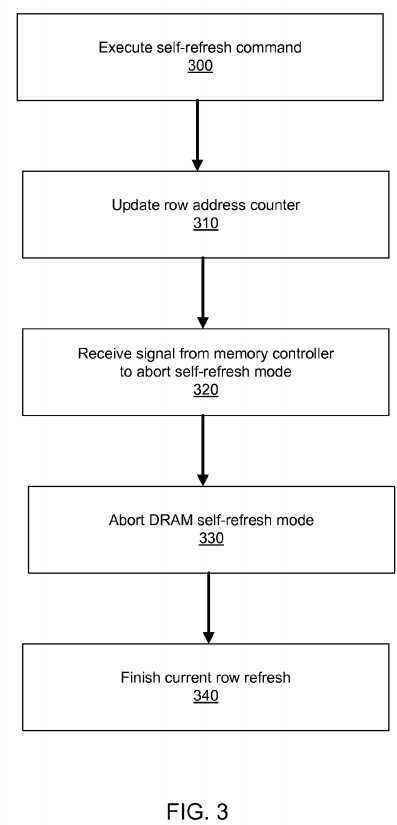
A self refresh mode is executed on a DRAM device,?300. The self refresh mode may be a plurality of commands, each command to refresh a plurality of rows of the DRAM device (e.g., 4 rows per command as described above).
The self-refresh mode may include commands to update a row address counter after each DRAM row is refreshed,?310. As describes above, the row address counter may indicate the rank, device and bank that includes the DRAM row that is to be refreshed.
An signal from a memory controller operatively coupled to the DRAM device indicating the self refresh mode is to be aborted may be received,?320. In one embodiment, this signal is a device enable signal. In other embodiments, the signal is a dedicated signal indicating the self-refresh mode is to be exited. The self-refresh mode is aborted in response to receiving the signal,?330. The DRAM device may include a self-refresh exit routine to handle self-refresh aborts consistently.
When the signal from the memory controller is received, it is possible that a self refresh was ongoing within the DRAM. If self-refresh was ongoing, then in one embodiment the self-refresh is aborted on a row boundary. In other words, the rows that are currently being refreshed are finished, but the row address counter is not incremented,?340.
For example, if DRAM was in the middle of refreshing the second of four rows, then row address counter bits [B01:B00] are at (0,1) assuming counters are incremented at end of refresh. In this embodiment, the 3rd and 4th row are not refreshed and row address counter bits [B01:B00] are reset to (0,0). Row address counters bits [B14:B2] are at the same value as before the refresh command that was aborted. In other words, they are not incremented. In other embodiments, row address counter bits [B01:B00] are incremented to reflect the last specific row that was refreshed before the self-refresh mode was aborted.
Thus, it is understood that in embodiments of the invention, due to the possibility of several aborts, the rows of a DRAM device may not be refreshed via the DRAM device self-refresh mode. The memory controller may initiate an external refresh to keep the data in the cells valid.
FIG. 4?illustrates a DRAM refresh cycle according to an embodiment of the invention. This diagram shows a potential self-refresh cycle for four rows of a bank according to an embodiment of the invention.
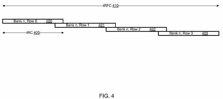
In this embodiment, a refresh command will refresh rows?400-403. The time to complete this command is represented by tRFC?410, while the time to complete a refresh of each row is represented by tRC?420.
It is to be understood that the fast self-refresh exit time in embodiments of the invention is tRC?420?(plus a guard band) as opposed to tRFC?410?(plus a guard band). As illustrated in?FIG. 4, tRC?420?is significantly shorter than tRFC?410. In this example, a 2 GBit DRAM devices a presumed, and thus tRC is 45 ns while tRFC is 160 ns. It is understood that the discrepancy between tRC and tRFC in high density DRAM devices is larger (e.g., tRFC for a 4 GBit device is in the range of 300 ns, while tRFC for an 8 Gbit device is in the range of 550 ns).
In one embodiment, a memory controller will at least periodically issue an extra DRAM device refresh command upon causing a DRAM device to exit the self-refresh mode. This ensures that all rows of a DRAM device are refreshed in the presence of a plurality of self-refresh mode aborts.
SRC=https://www.google.com.hk/patents/US20120079182
Fast exit from dram self-refresh,布布扣,bubuko.com
Fast exit from dram self-refresh
标签:des style blog http color os
原文地址:http://www.cnblogs.com/coryxie/p/3861936.html