码迷,mamicode.com
首页 > 其他好文 > 详细

[ASIC]Data Synchronization

时间:2016-01-13 09:20:38      阅读:187      评论:0      收藏:0      [点我收藏+]

标签:

Data Synchronization with Two Same-frequency/Different Phase Clock domains


When data is transferred from one clock domain to another clock domain, and the two clock domains are at the same clock-frequency, and are different clock phase for the two clock domain has different clock tree as show below.

技术分享

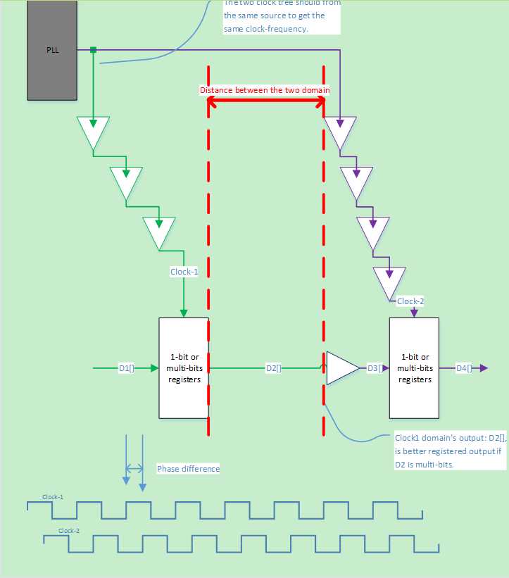
From the figure, there are several important points to be highlighted.

  1. The two      clock domain‘s clock tree should be the same source;
    1. Same PLL‘s       output;
    2. Different PLL, but same       clock reference;
  2. If D is multi-bits data, D      should be better registered-output from clock domain-1 (thus it is easier      for backend to balance the timing of D2[] and D3[] by adding less      buffers);
    1. From       experience, there is no must-to-have such requirement if D1 and D4 are       nearer in the floorplan of the design;
    2. If there is registers for       D2[], then the two clock domain can have long distance location, thus the       clock tree for the two clock domain will have clean boundary for dynamic       clock management and without introducing much power of buffers for       clock-tree‘s balance.
  3. Between D2[] and D3[],      balance buffer are added to meet the timing requirement for clock-2;


This method is benefit area comparing to a-sync-FIFO (the depth should be larger than 8) strategy for both 1-bit and multi-bits width data-synchronization. But the synthesis constraint should be put to the top-level of the 2 clock domains; and timing analysis should be very focus on this.

[ASIC]Data Synchronization

标签:

原文地址:http://www.cnblogs.com/zhuzhengchao/p/5126209.html

(0)
(0)
   
举报
评论 一句话评论(0
登录后才能评论!
© 2014 mamicode.com 版权所有  联系我们:gaon5@hotmail.com
迷上了代码!