标签:des style blog http color os strong io
Solid-state storage management for a system, the management including establishing, externally to a solid-state storage board, a correspondence between a first logical address and a first physical address on solid-state storage devices located on the solid-state storage board. The solid-state storage devices include a plurality of physical memory locations identified by physical addresses. The correspondence between the first logical address and the first physical address is accepted by the solid-state storage board. The correspondence between the first logical address and the first physical address is stored in a location on a solid-state memory device that is accessible by an address translator module, the address translator module and the solid-state memory device located on the solid-state storage board. The first logical address is translated to the first physical address by the address translator module based on the previously established correspondence between the first logical address and the first physical address.
The present invention relates to computer storage, and more specifically, to solid-state storage management.
Solid-state drives (SSDs) are data storage devices that use solid-state memory to store persistent data. SSDs are most commonly connected to a host computer via a high speed link. SSDs usually implement some form of management of the storage medium, i.e., the underlying solid-state storage devices. Such management usually includes translating from a logical address space into a physical address space. Many SSDs use "not-and" (NAND) based flash memory which must be erased in blocks before being rewritten with new data. Address translation is commonly used with NAND flash devices due to the difficulty of erase operations.
In some contemporary systems that use NAND flash devices, all of the management functionality is performed on the host computer. In these systems, the address translation table is placed in the main memory of the host computer such that during a read operation the host computer determines the physical address corresponding to the logical read address (address translation). During a write operation, the host computer decides the physical write address to which the data is written (physical data placement), and logs the logical-to-physical address correspondence in the address translation table. A shortcoming of this approach is that it requires the expenditure of computational cycles and main memory at the host in order to perform the address translation. Thus, it is well-suited for computer systems with large amounts of dynamic random access memory (DRAM) and processing capabilities, and is not well suited for lower cost systems with limited amounts of DRAM and processing capabilities, or for large-scale data-centric systems with high ratios between storage and system memory.
Other contemporary systems place all of the management functionality on the physical SSD board. In this case, SSD does both data placement and address translation. A shortcoming of this approach is that it suffers in terms of cost/performance because it does not leverage the host processor and instead requires another processor to be incorporated into the SSD.
An embodiment is a system that includes a main board and a solid-state storage board separate from the main board. The main board is coupled to the solid-state storage board via an interface bus. The solid-state storage board includes a solid-state memory device and solid-state storage devices. The solid-state storage devices include a plurality of physical memory locations identified by physical addresses. The system is configured to perform a method that includes establishing a correspondence between a first logical address and a first physical address on the solid-state storage devices. The establishing is by a software module located on the main board. The correspondence between the first logical address and the first physical address is stored in a location on the solid-state memory device located on the solid-state storage board. The method also includes translating the first logical address into the first physical address. The translating is performed by an address translator module located on the solid-state storage board and is based on the previously established correspondence between the first logical address and the first physical address.
Other embodiments include a method and computer program product for establishing a correspondence between a first logical address and a first physical address on solid-state storage devices located on solid-state storage board. The solid-state storage devices include a plurality of physical memory locations identified by physical addresses, and the establishing is by a software module located on a main board that is separate from the solid-state storage board. The main board is coupled to the solid-state storage board via an interface bus. The correspondence between the first logical address and the first physical address is stored in a location on a solid-state memory device that is accessible by an address translator module located on the solid-state storage board. The solid-state memory device is located on the solid-state storage board. The first logical address is translated to the first physical address by the address translator module based on the previously established correspondence between the first logical address and the first physical address.
Embodiments of the present invention provide high performance solid-state drive (SSD) management solutions for use with low-cost or large-scale data-centric computer systems. Specifically, embodiments include an innovative split of flash memory management complexity between a host system and a SSD board, also referred to herein as a hardware module or solid-state storage board. In particular, a host system processor executes a software module that utilizes system resources to perform a specific subset of the tasks involved in SSD management, whereas the remaining tasks are performed and accelerated directly by the SSD board. The hardware module incorporates a controller sub-module, as well as "not-and" (NAND) flash memory and some high speed memory such as dynamic random access memory (DRAM), phase-change memory (PCM) and/or spin-torque transfer random access memory (STT-RAM). The software module handles complex flash memory management operations including, but not limited to: garbage collection, wear leveling, data placement and scheduling, second-tier error correction coding (ECC), redundant array of independent disks (RAID) management, and flash recovery. On the other hand, the hardware controller module handles simple flash translation layer (FTL) bookkeeping (the FTL is the address translation table in NAND-flash systems) and flash command routing, as well as hardware friendly operations such as RAID acceleration and primary-tier ECC using algebraic codes.
Embodiments described herein have very small footprints on the host system and processor in terms of processing power and host memory. Even the most complex flash bookkeeping operations require only a fraction of the computing power of a typical modern host processor, whereas full flash management has a significant impact on system memory occupancy and, as a consequence system performance. Thus, embodiments can be used in systems with inexpensive memory subsystems and relatively inexpensive processors, or systems where power efficiency is a top priority and most of the memory resources will be claimed by the main user application, or large-scale data-centric systems which use several low power compute nodes and/or micro-servers. In addition, the simple hardware module allows low latency and large bandwidth FTL transactions and delivery of flash commands to the flash memory devices. Thus, even on systems running independent concurrent high throughput memory intensive applications, the system and method allows very high performance to be attained. Further, due to the simplicity of hardware this performance is achieved at relatively low costs. The cost/performance of exemplary embodiments in terms of cost/gigabytes (GB), for example, or cost/bandwidth, is significantly better than conventional solutions. Embodiments described herein are well suited for providing high performance at a low cost for systems with limited available resources.
Turning now to?FIG. 1, an embodiment of a flash controller system is generally shown. The system includes a host computer?100?connected or coupled to a hardware module?102?by an interface?104. In an embodiment, the host computer100?is a computer system with a main board and a connection to one or more high-speed buses that serve as the interface104?to the hardware module?102. The host computer?100?includes hardware located on the main board (e.g., a motherboard), such as a processor and memory, that execute software, including software module?106. In an embodiment, the software module?106?is responsible for most of the complex flash controller management functions such as garbage collection, wear leveling, optimizing data placement and scheduling, RAID management, flash disaster recovery and higher layer ECC functionality.
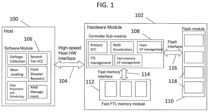
In an embodiment, the hardware module?102?is a physical device and responsible primarily for housing a flash module?110, a controller sub-module?108?and a fast memory module?112. Herein, the terms "hardware module" and "solid-state storage board" are used interchangeably. In an embodiment, the controller sub-module?108?accesses the FTL, which resides in one or more solid-state memory devices such as a DRAM?112?or some other high speed volatile or nonvolatile memory on the hardware module?102. As known in the art, the FTL includes a mapping between logical addresses and physical addresses. The flash module?110?includes flash memory devices (e.g., chips)?118?that reside on the hardware module?102. A flash memory device is an example of one type of solid-state storage device that may be implemented by exemplary embodiments. Other examples of solid-state storage devices that may be implemented include PCM, magnetic RAM and resistive RAM.
The main functions of the hardware module?102?include the efficient translation of logical-to-physical addresses to facilitate reading from the flash memory devices?118, and low latency and high bandwidth delivery of flash commands to the flash memory devices?118. To this end, the hardware module?102?also incorporates interface management functions, which manage a fast memory interface?114?between a fast FTL memory module?112?and the flash module?110. In addition, the hardware module?102?is responsible for some simple operations suitable for hardware acceleration, that run on the controller sub-module?108?such as primary error correction code (ECC) and some RAID acceleration operations. The controller sub-module?108?is connected to the flash module?110?via a flash interface?116. In addition, the hardware module102?facilitates the recovery of physical-to-logical address mapping to enable effective operation of management algorithms, including data placement and garbage collection algorithms, as performed by the software module?106. In an embodiment, the hardware module?102?and software module?106?on the host computer?100?are interconnected using interface?104. In an embodiment, interface?104?is a high-speed host hardware interface, such as a high-speed Peripheral Component Interconnect Express (PCIe) interface.
The embodiment depicted in?FIG. 1?for SSD management utilizes an innovative split of flash controller management functionality between the software module?106?(e.g., a driver executing on the host computer?100) and the hardware module?102?(e.g., executing on a card with suitable hardware, such as a field programmable gate array or "FPGA", or a controller application specific integrated circuit or "ASIC"). In an embodiment, hardware for acceleration of specific functionalities such as ECC and a table used for translation between logical addresses and physical addresses are in the hardware module?102, and flash management processes such as data placement, wear leveling and control (e.g., based on a wear measurement), and garbage collection, and metadata such as wear data and page status are in the host computer100. The simplicity of the arrangement and hardware reduces both the cost of the required host computer system and the complexity of the design of hardware module?102. For example, in the embodiment depicted in?FIG. 1?the hardware module does not need to implement generic processor core functionality, as commonly done in the art.
The split of the flash controller functionality between the host computer?100?and hardware module?102?allows very high performance to be attained. This is due to the software module?106?on the host computer?100?controlling the complex flash operations, where the host computer?100?has sufficient computing system resources for the operations. This is in contrast to performing complex flash operations entirely on the hardware module?102, where resources on the hardware module?102may cause a bottleneck for complex operations. The arrangement depicted in?FIG. 1?also saves costly system resources, such as main memory on the host computer?100, by placing the FTL memory module?112?on the hardware module?102. Thus, embodiments are used to facilitate high performance flash I/O in new applications, such as micro-servers in data-center networking, where system resources such as main memory are constrained, and allow accelerated development due to the simplicity of the hardware module?102. A description of how exemplary flash operations are performed according to embodiments is shown in?FIGS. 2-6.
FIG. 2?is a block diagram of a process for performing a read flash operation (also called read logical address flash operation) according to an embodiment. In a first block?200, a user read request for a SSD, such as a flash memory device118, is received by the host computer?100. At block?202, the read request is split into physical read units, where each unit has its own logical address. The requests are then queued to an outbound request queue in block?204. At block?206, the hardware module?102?is checked, either directly, or by inferring its status given the previous history of commands and requests and the capabilities of the hardware module?102?itself, to see if it is cleared to send (CTS) the read requests. The hardware module?102?indicates CTS if it is free to perform or accept commands. If the hardware module?102?is CTS, the requests are sent to the hardware module?102, as shown in block?208. In block?210, if the module is not cleared, the system will wait until the hardware module?102?indicates it is clear. In an embodiment, blocks?200-210?are performed by the host computer?100, and blocks?212-220?are performed by the hardware module?102.
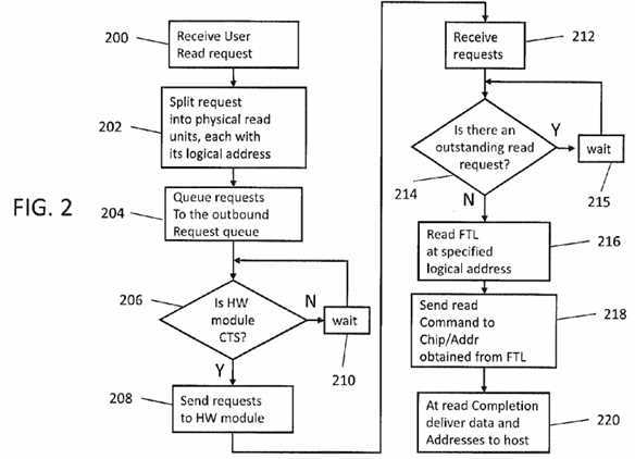
In block?212, the read requests for each of the logical addresses are received. In block?214, the hardware module?102determines if there is an outstanding read request, for example at the same hardware resource (possible hardware resources include a flash module, a memory device or chip, a die, of plane) where the read operation has to be performed. If there are outstanding read requests, the module waits, as shown in block?215. If there are no outstanding read requests, block?216?is performed to read the fast FTL memory module?112?(also referred to as "FTL") at the specified logical address to determine the physical address that corresponds to the logical address. At block?218, a read command is sent to the physical address obtained from the FTL. The FTL performs the translation of the logical address to the physical address on the hardware module?102. In block?220, after the read is completed, the data is delivered along with the logical address by the hardware module?102?to the host computer?100?via the interface?104. In another embodiment, the physical address is also sent to the host computer?100?via the interface.
FIG. 3?is a block diagram of a process for a write flash operation according to an embodiment. At block?300, the host computer?100?receives a user write request. In block?302, the write request is split into physical write units, where each unit has a logical address. At block?304, a data placement algorithm obtains a physical address for each logical address. The data placement algorithm executes on the host computer?100?software module?106?and determines the physical address based on selected data (e.g., metadata) on the host computer?100, such as wear information and other flash device information. In an embodiment, the physical write location determined by the placement algorithm is selected so as to equalize wear across different physical locations, using determination algorithms well known in the art. In another embodiment, the physical location determined by the placement algorithm is such as to reduce write amplification from future garbage collection operations; the algorithms to determine such a physical location are well-known in the art. In another embodiment the solid-state storage devices include a mixture of devices with different performance characteristics, for example single-level cell (SLC) and multi-level cell (MLC) flash. In this case the placement algorithm takes the physical characteristics of devices into account while determining the physical location. For example, data that is expected to be rewritten frequently is placed on a high-endurance device such as SLC flash, while infrequently updated data is placed on low-endurance devices such as MLC flash. In an embodiment, establishing a correspondence between a logical address and a physical address is responsive to at least one of a measurement of wear of at least one of the solid-state storage devices, projected performance of the main board, and characteristics of at least one of the solid-state storage devices. In an embodiment, establishing a correspondence between a logical address and a physical address is responsive to prior output of an ECC decoder. Thus, information about the location of prior errors is taken into account when deciding on a physical location for the data.
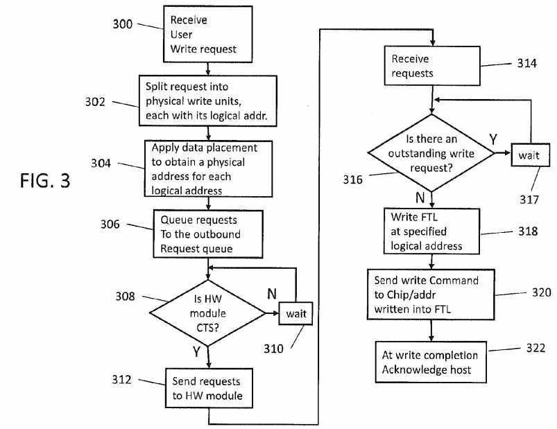
The requests are then queued at an outbound request queue in block?306. In block?308, the hardware module?102?is checked to see if it is CTS the write requests. In block?310, if the module is not cleared, the system will wait until the hardware module?102?indicates it is clear. If the hardware module?102?is CTS, the requests, including the data to be written along with the logical and physical addresses, are sent to the hardware module?102, as shown in block?312. In an embodiment, blocks?300-312?are performed by the host computer?100, and blocks?314-322?are performed by the hardware module?102.
At block?314, the write requests for each of the logical and physical addresses are received. In block?316, the hardware module?102?determines if there are outstanding write requests, for example at the same hardware resource (possible hardware resources include a flash module, a memory device or chip, a die, of plane) where the write operation has to be performed. If there are outstanding write requests, the module waits, as shown in block?317. If there are no outstanding write requests, the hardware module?102?writes to update the FTL at the specified logical address for each physical address, as shown in block?318. At block?320, the write command is sent to the flash memory device or physical address of the memory, where the physical address matches the address written into the FTL in block?318. In block?322, a write completion acknowledgement is sent to the host computer?100.
FIG. 4?is a block diagram of process for a garbage collection operation in accordance with an embodiment. At block?400, the host computer?100?finds the best candidate block of data to erase during the operation. In an embodiment, the best candidate is the block with the least number of valid pages. In another embodiment, the candidate is selected because it has the least amount of wear. The host computer?100?may use metadata and other information stored on the host computer100?that describes flash memory properties to identify the candidate for the erasing operation. Further, the metadata on the host computer?100?also provides the physical addresses of the block of data selected for erasing. Metadata stored at the host includes one or more of the following: valid status of each physical page, status of each block, possibly including current write page, erase status, erase count, either precise or approximate, and current operation being performed if any. In an embodiment this information is processed by an independent thread of execution. In additional embodiments this information is processed when a garbage collection operation is triggered.
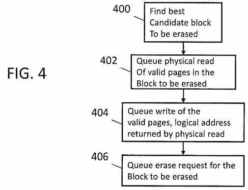
At block?402, a read physical address flash operation, such as that described below in?FIG. 5, is queued for any valid pages within the block of data identified at block?400. In an embodiment, the physical addresses of the valid pages are determined using an offset value from the starting physical address of the block of data to be erased by the garbage collection process. The physical addresses of the valid pages to be erased are queued, and at block?404, the write of the valid pages and logical addresses returned by the physical read are queued. The logical address associated to a physical page is obtained from metadata appended to the page contents at write time and retrieved alongside with the page contents when performing a read operation. At block?406, the erase requests for the block of data to be erased are queued after all the valid pages have been written (i.e., copied) in block?404?to another location. The process maintains the logical address as the physical addresses of valid pages are changed, where the FTL is updated with the new address for the data. In an embodiment, the processing depicted in?FIG. 4?is performed by the host computer?100.
FIG. 5?is a block diagram of a process for a read physical address flash operation according to an embodiment. At block500, a request for reading data from a physical address is queued to the outbound request queue of the host computer100. At block?502, the hardware module?102?is checked to see if it is CTS the read requests. At block?506, if the module is not cleared, the system will wait until the hardware module?102?indicates it is clear. If the hardware module?102?is cleared to send, the read requests and corresponding physical addresses are sent to the hardware module?102, as shown in block504. In an embodiment, blocks?500-504?are performed by the host computer?100, and blocks?508-514?are performed by the hardware module?102.
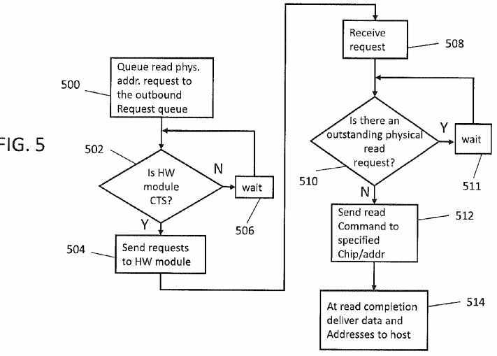
In block?508, the read requests for each of the physical addresses are received. At block?510, the hardware module?102determines if there is an outstanding physical address read request. If there are outstanding read requests, the module waits, as shown in block?511. If there are no outstanding requests, the read command is sent to the specified physical address in block?512. After the data has been read at the specified physical address, the data and the logical address are delivered to the host computer?100?by the hardware module?102. The read physical address operation may be performed when the host computer?100?knows the physical address of the data it is requesting, such as for a garbage collection operation as described above in?FIG. 4.
In additional exemplary embodiments, only an acknowledgment is provided to the host computer?100?after the data is read. The read data is stored on the hardware module?102, for example in a buffer on the controller sub-module?108?or in other memory available at the hardware module?102. In additional embodiments the logical address associated with the page read is communicated back to the host computer?100. In additional embodiments the logical address is stored in a buffer available at the hardware module?102. Whenever the data is stored in a buffer at the hardware module?102, the write operation required to save the page to be erased does not include transferring the page data from the host computer?100, but only requesting that the data used in the write operation is obtained from the buffer at hardware module?102.
FIG. 6?is a block diagram of a process for a flash erase operation according to an embodiment. At block?600, a physical address of the block of data in the flash to be erased is obtained. At block?602, the erase request is sent to the outbound request queue. At block?604, the hardware module?102?is checked to see if it is CTS the erase request. At block?608, if the module is not cleared, the system will wait until the hardware module?102?indicates it is clear. If the hardware module?102?is cleared to send, the erase requests and corresponding physical addresses are sent to the hardware module?102, as shown in block?610. In an embodiment, blocks?600,?602,?604,?608?and?610?are all performed by the host computer?100, and blocks?612,?614,?616?and?618?are performed by the hardware module?102.
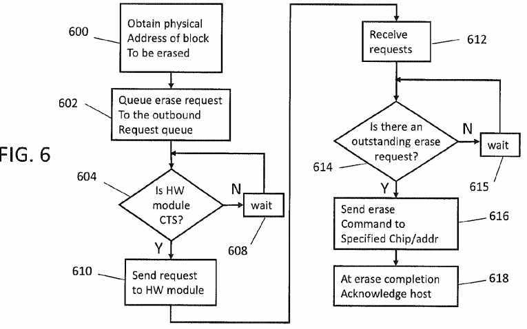
At block?612, the erase requests for each of the physical addresses are received. At block?614, the hardware module?102determines if there is an outstanding erase requests. If there are no outstanding erase requests, the module waits, as shown in block?615. If there is an outstanding request, the erase command is sent to the specified physical address and flash memory device?118?at block?616. After the data has been erased at the specified physical address, an acknowledgement of the erased data is communicated to the host computer?100?by the hardware module?102. The erase operation may be performed when the host computer knows the physical address of the data it is requesting to erase, such as for a garbage collection operation as described above in?FIG. 4.
Embodiments provide a high performance solid-state device management solution that can be used with low cost volume processors. Specifically, embodiments include a split of flash management complexity between a software module running on a host processor and a hardware module that includes the flash memory. In embodiments, the host processor and system are located on a main board of a computer system which the hardware module is a card that includes the flash memory, a controller sub-module and a fast memory module. The fast memory module (including the FTL) on the hardware module hosts information used for logical to physical address translation (e.g., a table) to provide fast read operation performance. By placing the address translation information on the hardware module, valuable memory on the host is saved. Other metadata describing the flash memory is located on the host to utilize the host processor. Operations performed on the host using the metadata on the host utilize the host processor and do not negatively impact the performance of the hardware controller connected to the flash. The division of data and operations between the host and hardware module also simplifies the system while reducing cost by not having a processor on the module.
SRC=http://www.google.com/patents/US20140136769
Solid-state storage management,布布扣,bubuko.com
Solid-state storage management
标签:des style blog http color os strong io
原文地址:http://www.cnblogs.com/coryxie/p/3891163.html