标签:
RTL结构图
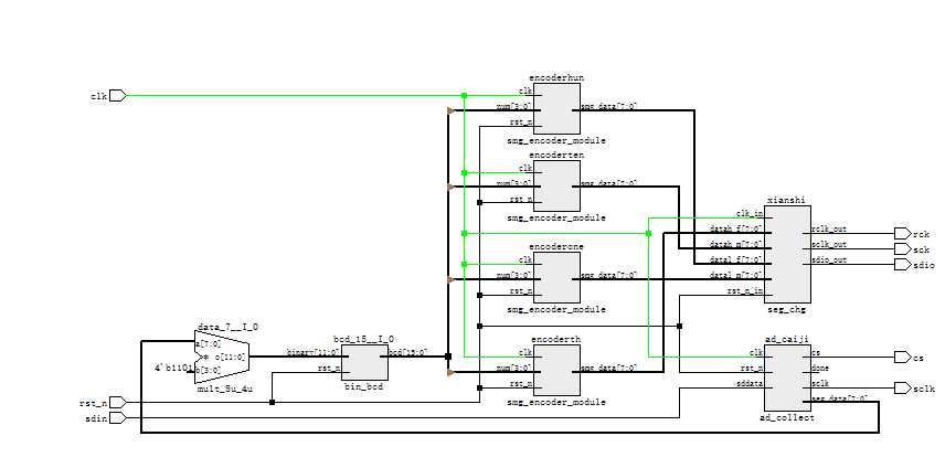
采集模块运用SPI 通讯 MISO方式收集数据
module ad_collect
(
input sddata,
input rst_n,
output reg cs,
output reg sclk,
input clk,
output [7:0]seg_data,
output done
);
reg [7:0]cnt;
reg[4:0]state;
reg[7:0]data;
reg rdone;
always@(posedge clk or negedge rst_n ) begin
if(cs==0)begin sclk<=!sclk; cnt<=cnt+1;end
if(!rst_n)begin cs<=1;state<=0;cnt<=0;sclk<=1;rdone=0;end
else
begin
case(state)
0:if(rst_n==1)begin cs<=0;state<=state+1;end
1:if(cnt==8) begin data[7]<=sddata;state<=state+1;rdone=0;end
2:if(cnt==10) begin data[6]<=sddata;state<=state+1;rdone=0;end
3:if(cnt==12) begin data[5]<=sddata;state<=state+1;rdone=0;end
4:if(cnt==14) begin data[4]<=sddata;state<=state+1;rdone=0;end
5:if(cnt==16) begin data[3]<=sddata;state<=state+1;rdone=0;end
6:if(cnt==18) begin data[2]<=sddata;state<=state+1;rdone=0;end
7:if(cnt==20) begin data[1]<=sddata;state<=state+1;rdone=0;end
8:if(cnt==22) begin data[0]<=sddata;;state<=state+1;rdone=0;end
9:if(cnt==32) begin cs<=1;state<=state+1;sclk<=0;rdone=1;end
10: begin cnt<=cnt+1;if(cnt==42)begin cnt<=0;state<=0;rdone=0;end end
endcase
end
end
assign done=rdone;
assign seg_data=rdone?data[7:0]:seg_data;
endmodule
将输出的8位255的BCD码对应成3.3V的显示,用输出的Q[7:0]去乘上13,给二进制转BCD模块,最后数码管显示控制小数点的位置相当于再除以1000。
//这是一个使用Verilog HDL编写的带使能端的8-bit二进制转BCD码程序,具有占用资源少、移植性好、扩展方便的特点。
/********************************************\
Filrst_nme : B_BCD.v Author : Medied.Lee
Description : a 8-bit binary-to-bcd module
Revision : 2010/11/20 Company :
\********************************************/
module bin_bcd(rst_n,binary,bcd);
//rst_n为使能端,binary为待转换的二进制数,bcd为转换后的BCD码
parameter B_SIZE=12;
//B_SIZE为二进制数所占的位数,可根据需要进行扩展
input binary,rst_n;//rst_n高电平有效,低电平时
output bcd;
wire rst_n;
wire [B_SIZE-1:0] binary;
reg [B_SIZE-1:0] bin;
reg [B_SIZE+3:0] bcd; // bcd的长度应根据实际情况进行修改
reg [B_SIZE+3:0] result; //result的长度=bcd的长度
always@(binary or rst_n)
begin
bin= binary;
result = 0;
if(rst_n == 0)
bcd <= 0;
else
begin
repeat(B_SIZE-1)//使用repeat语句进行循环计算
begin
result[0] = bin[B_SIZE-1];
if ( result[3:0] > 4 )
result[3:0]=result[3:0]+ 4‘d3;
if(result[7:4]> 4)
result[7:4]=result[7:4]+4‘d3;
if(result[11:8]>4)
result[11:8] = result[11:8]+4‘d3;
//扩展时应参照此三条if语句续写
if(result[15:12]>4)
result[15:12]= result[15:12]+ 4‘d3;
result=result<<1;
bin=bin<<1; end
result[0]= bin[B_SIZE-1];
bcd<=result;
end
end
endmodule
输出的结果经过数码管译码
module smg_encoder_module(clk,rst_n,num,smg_data);
input clk;
input rst_n;
input [3:0]num;
output [7:0]smg_data;
/*共阴极数码管: 位选为低电平(即0)选中数码管; 各段选为高电平(即1接+5V时)选中各数码段;*/
//由0到f的编码为
parameter
SEG_NUM0=8‘h3f,
SEG_NUM1=8‘h06,
SEG_NUM2=8‘h5b,
SEG_NUM3=8‘h4f,
SEG_NUM4=8‘h66,
SEG_NUM5=8‘h6d,
SEG_NUM6=8‘h7d,
SEG_NUM7=8‘h07,
SEG_NUM8=8‘h7f,
SEG_NUM9=8‘h6f,
SEG_NUMA=8‘h77,
SEG_NUMB=8‘h7c,
SEG_NUMC=8‘h39,
SEG_NUMD=8‘h5e,
SEG_NUME=8‘h79,
SEG_NUMF=8‘h71;
reg [7:0]smg_data_r;
always @(posedge clk or negedge rst_n)
begin
if(!rst_n)
smg_data_r <= 8‘b00000000;
else
case (num)
4‘d0: smg_data_r <= SEG_NUM0;
4‘d1: smg_data_r <= SEG_NUM1;
4‘d2: smg_data_r <= SEG_NUM2;
4‘d3: smg_data_r <= SEG_NUM3;
4‘d4: smg_data_r <= SEG_NUM4;
4‘d5: smg_data_r <= SEG_NUM5;
4‘d6: smg_data_r <= SEG_NUM6;
4‘d7: smg_data_r <= SEG_NUM7;
4‘d8: smg_data_r <= SEG_NUM8;
4‘d9: smg_data_r <= SEG_NUM9;
default: smg_data_r <= 8‘b00000000;
endcase
end
assign smg_data=smg_data_r;
endmodule
最后经过串行数据发送数据给595输出
module seg_chg
(
input clk_in, //25mhz
input rst_n_in, //active with low
input [7:0] datah_f,
input [7:0] datal_f,
input [7:0] datah_m,
input [7:0] datal_m,
output reg rclk_out, //74HC595 RCK
output reg sclk_out, //74HC595 SCK
output reg sdio_out //74HC595 SER
);
parameter CLK_DIV_PERIOD=3900; //related with clk_div‘s frequency
parameter DELAY_PERIOD=10000; //related with delay time and refresh frequency
parameter CLK_DIV_PULSE_PERIOD=25000000; //related with clk_div_pulse_out‘s frequency
parameter CLK_L=2‘d0;
parameter CLK_H=2‘d1;
parameter CLK_RISING_DEGE=2‘d2;
parameter CLK_FALLING_DEGE=2‘d3;
parameter IDLE=3‘d0;
parameter WRITE=3‘d1;
parameter DELAY=3‘d2;
parameter LOW =1‘b0;
parameter HIGH =1‘b1;
//initial for memory register
reg[24:0] cnt;
reg clk_div_1Hz;
always@(posedge clk_in or negedge rst_n_in)
begin
if(!rst_n_in) begin
cnt<=0;
clk_div_1Hz<=0;
end else if(cnt==(CLK_DIV_PULSE_PERIOD-1)) begin
cnt<=0;
clk_div_1Hz<=1;
end else begin
cnt<=cnt+1;
clk_div_1Hz<=0;
end
end
//clk_div = clk_in/CLK_DIV_PERIOD
reg clk_div;
reg[11:0] clk_cnt=0;
always@(posedge clk_in or negedge rst_n_in) begin
if(!rst_n_in) clk_cnt<=0;
else begin
clk_cnt<=clk_cnt+1;
if(clk_cnt==(CLK_DIV_PERIOD-1)) clk_cnt<=0;
if(clk_cnt<(CLK_DIV_PERIOD/2)) clk_div<=0;
else clk_div<=1;
end
end
//Divide clk_div 4 state,
//RISING and FALLING state is keeped one cycle of clk_in, like a pulse.
reg[1:0] clk_div_state=CLK_L;
always@(posedge clk_in or negedge rst_n_in) begin
if(!rst_n_in) clk_div_state<=CLK_L;
else case(clk_div_state)
CLK_L: begin
if (clk_div) clk_div_state<=CLK_RISING_DEGE;
else clk_div_state<=CLK_L;
end
CLK_RISING_DEGE :clk_div_state<=CLK_H;
CLK_H:begin
if (!clk_div) clk_div_state<=CLK_FALLING_DEGE;
else clk_div_state<=CLK_H;
end
CLK_FALLING_DEGE:clk_div_state<=CLK_L;
default;
endcase
end
//Finite State Machine,
reg shift_flag = 0;
reg[15:0] data_reg;
reg[2:0] data_state=IDLE;
reg[2:0] data_state_back;
reg[3:0] data_state_cnt=0;
reg[5:0] shift_cnt=0;
reg[25:0] delay_cnt=0;
always@(posedge clk_in or negedge rst_n_in) begin
if(!rst_n_in) begin
data_state<=IDLE;
data_state_cnt<=0;
end else begin
case (data_state)
IDLE: begin
data_state_cnt<=data_state_cnt+1;
case(data_state_cnt)
0: begin
data_reg<={{1‘b1,datah_f[6:0]}, 8‘h0e};
data_state<=WRITE;data_state_back<=IDLE;
end
1: begin
data_reg<={datal_f,8‘h0d};
data_state<=WRITE;data_state_back<=IDLE;
end
2: begin
data_reg<={datah_m,8‘h0b};
data_state<=WRITE;data_state_back<=IDLE;
end
3: begin
data_reg<={datal_m,8‘h07};
data_state<=WRITE;data_state_back<=IDLE;
end
4: begin data_state_cnt<=0; end
default;
endcase
end
WRITE: begin
if(!shift_flag) begin
if (clk_div_state==CLK_FALLING_DEGE) begin
if (shift_cnt==10) rclk_out<=LOW;
if (shift_cnt==16) begin
shift_cnt<=0;
rclk_out<=HIGH;
data_state<=data_state_back;
end else begin
sclk_out<=LOW;
sdio_out<=data_reg[15];
shift_flag <= 1;
end
end
end else begin
if (clk_div_state==CLK_RISING_DEGE) begin
data_reg<={data_reg[14:0], data_reg[15]};
shift_cnt<=shift_cnt+1;
sclk_out<=HIGH;
shift_flag <= 0;
end
end
end
DELAY: begin
if(delay_cnt==DELAY_PERIOD) begin
data_state<=IDLE;
delay_cnt<=0;
end else delay_cnt<=delay_cnt+1;
end
default;
endcase
end
end
endmodule
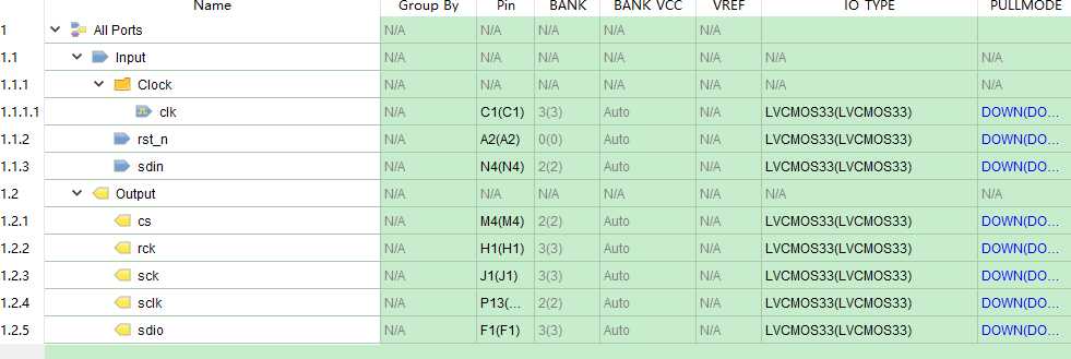
管脚分配
http://stepfpga.ecbcamp.com/doc/%E7%9B%B4%E6%B5%81%E7%94%B5%E5%8E%8B%E6%B5%8B%E9%87%8F 相关资料
标签:
原文地址:http://www.cnblogs.com/xinshuwei/p/5647878.html