标签:ecif tps seconds time tput ide AMM line which
用DS12C887设计一个万年历,虽然反复查看说明书,还是出各种的错误。
因此,从美信官网查询资料,翻译的不太通,凑合着对照看。
Tips for Writing Bulletproof Real-Time Clock Control Code
关于编写健壮的实时时钟控制代码的提示
摘要 : With the use of proper device initialization and code sequencing, accurate timekeeping and clock alarm operations become a more manageable task.
摘要:正确使用设备初始化和代码顺序,使得精确计时和闹钟成为一项更易于管理的任务。
Introduction
介绍
When we read a clock, as we have all done since childhood, our eyes ‘take a snapshot‘ of the present displayed values. Someone has already gone through the effort to reorient that display for your readability. When the microprocessor needs to access the real-time clock, the ‘snapshot‘ of the latest register values must be reoriented into a sequence of time counts that we are more familiar with.
就像小时候看表时,我们的眼睛扫一下显示的值。为了更加易读,有人已努力调整了显示的方式。当微处理器需要访问实时时钟时,必须将寄存器最新值的“快照”重新定向到我们比较熟悉的一系列时间值中。
With the use of proper device initialization and code sequencing, accurate timekeeping and clock alarm operations become a more manageable task.
正确的设备初始化和代码顺序,使得精确计时和闹钟成为一项更易于管理的任务。
Device Initialization
设备初始化
Upon the first power application to a new clock component, the sequence of required I/O instructions may vary, based upon that specific component. Refer to the device specification for register structuring. As a general guideline, and assuming power is stable and the I/O port is operational, it is recommended to:
首次使用新时钟组件,所需 I/O 指令的顺序可能因该特定组件而异。有关寄存器结构,请参阅设备规范。作为一般准则,假设电源稳定且 I/O 端口可运行,则建议:
Enable Writing to the RTC: This unique function was added to some component designs (for example, the DS1305) to prevent inadvertent clock changes. Refer to the product specification for the write-protect (WP) bit explanation.
启用芯片写入:此功能已添加到某些组件设计中(例如 DS1305),以防止时钟意外更改。有关书写保护位(WP)说明,请参阅产品规范。
Enable RTC Oscillator: On some legacy designs (such as DS12887, DS1307), the RTC oscillator does not auto-start at first power-up. This operational feature was intended to prevent battery consumption during transit/storage, and must be enabled through I/O. Designs with an %-overbar_pre%EOSC%-overbar_post% bit in the Control register include a built-in oscillator auto-start function, executed upon the first power application. In some other designs like DS1685, it may also be necessary to identify the crystal load capacitance setting for proper oscillator operation.
启用振荡器:在某些传统设计上(如DS12887,DS1307),振荡器在第一次上电时不会自动启动。此功能旨在防止在运输/存储期间消耗电池,必须通过 I/O开启。在控制寄存器中设有 %-overbar_pre%EOSC%-overbar_post% 位,包括内置振荡器自动启动功能,该功能在第一此上电时执行。在DS1685等其他设计中,可能还需要识别晶体负载电容设置,以便进行正确的振荡器操作。
Check ‘OSF‘: Some RTC components contain an oscillator stop flag (OSF), allowing the user to monitor oscillator operation via periodic I/O. Upon initial power application, OSF will be set. After enabling the oscillator, clear OSF, and then periodically verify that the OSF bit remains Logic 0.
检查"OSF":某些RTC元件包含振荡器停止标志(OSF),允许用户通过周期I/O监控振荡器操作。第一次上电时,OSF将被设置。启用振荡器后,会清除OSF,然后定期验证OSF位是否保持逻辑 0。
OSF may become Logic 1 based upon any of these conditions:
OSF 可能基于以下任一条件变为逻辑 1:
Define Interrupt Output(s): Depending upon the specific component and the desired application, definition of the output functions should now be executed to prevent unintended signals from being sent to the microprocessor. Component programming options for real-time alarm(s), watchdog interrupt, square-wave output frequency, etc., should be selected to establish the desired pin/signal conditioning.
定义中断输出:根据特定组件和所需应用,应定义中断输出功能,以防止意外信号发送到微处理器。应选择用于实时闹钟、看门狗中断、方波输出频率等的元件编程选项,以建立所需的引脚/信号节奏。
In devices with real-time alarms, every alarm register should initially be written to 00h (if binary-coded decimal (BCD)) or FFh (if binary) to prevent any inadvertent matching/interrupt generation. The alarm registers are not factory-initialized, and the associated alarm flags can appear at any time the alarm register contents match the real-time count.
在具有实时闹钟的设备中,每个闹钟寄存器最初应写入FFh(BCD模式)或00h(二进制模式),以防产生任何意外匹配/中断。闹钟寄存器未做出厂初始化,且实时计数与闹钟寄存器匹配时,设置闹钟标志。
Load Initial Counter (Time) Values: Again referring to the product‘s specification and register map, the order of counter loading or reading should be executed from least significant count to the most significant count. Figure 1 illustrates the counter orientation and carry functions for a typical BCD-formatted real-time clock component.
加载初始计数器(时间)值:再次参考产品说明书和寄存器映射,计数器加载或读取的顺序应执行“从最低位到最高位”的顺序。图 1 说明了典型 BCD 格式的实时时钟组件的逆向执行顺序。
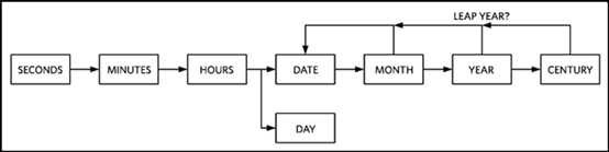
Figure 1. RTC counter chain. RTC计数链
Whenever writing to the RTC, any write to the least significant counter byte resets the internal 1Hz chain, allowing the user one full second before any timekeeping counter bits subsequently increment. This 1Hz reset action, as well as synchronization techniques, are explained in further detail in the Time Synchronization section.
写入时,对最低计数器(秒)的任何写入都会重置内部的1Hz链,以使用户在写入后,计时计数器位增加之前,有整整一秒的时间。此1Hz重置操作以及同步技术,在时间同步部分中作了更详细的说明。
To facilitate ease of use, the registers are oriented in ascending weight and address order for your programming convenience.
为了便于使用,寄存器以升序权重和地址顺序定向,以方便您的编程。
|
BCD Format |
Binary (Seconds) |
|
Hundredths of a Second (if so equipped) |
00h -> FFh = 0 -> 255. |
|
Seconds |
00h -> FFh = 256. -> 65535. |
|
Minutes |
00h -> FFh = 65536. -> 16777215. |
|
Hours |
00h -> FFh = 16777216. -> 4294967295. |
|
Day of Week |
|
|
Date |
|
|
Month |
|
|
Year |
|
|
Century (if so equipped) |
|
Time Synchronization
时间同步
To some users, the simple act of setting the clock (writing to the RTC) may accomplish the timekeeping accuracy goals for the real-time clock in that application. Depending upon the care taken when initializing our device, an initial clock-set error of a few seconds may be considered acceptable when weighed against the execution of the other tasks controlled by that application.
对于某些用户来说,设置时钟的简单操作(写入 RTC)可以完成实时时钟的计时精度目标。初始化设备时应小心谨慎,在与该应用程序控制的其他任务的执行量权衡时,几秒钟的初始时钟设置错误可能被认为是可以接受的。
In other applications, it may be desired to synchronize the real-time clock with a known time standard, like WWV1. As previously mentioned, writing to the least significant counter byte resets the 1Hz countdown chain. Figure 2 illustrates how to reset the 1Hz countdown chain using an I2C Write sequence to the SECONDS register of a DS1340. The slave address byte (D0h), register address (00h), and ‘updated Seconds value‘ (03h), are being transmitted to the component. Two representative examples of an asynchronous 1Hz square-wave output are shown to illustrate the resulting adjustment.
在其他应用中,可能需要将实时时钟与已知时间标准(如 WWV1)同步。如前所述,写入最低显著计数器字节将重置 1Hz 倒计时链。图2说明了如何使用I2 C写入序列将DS1340的秒寄存器1Hz倒计时链重置。从地址字节(D0h)、寄存器地址(00h)和"更新的秒值"(03h)正在传输到组件。显示了两个异步 1Hz 方波输出的代表性示例,以说明调整结果。
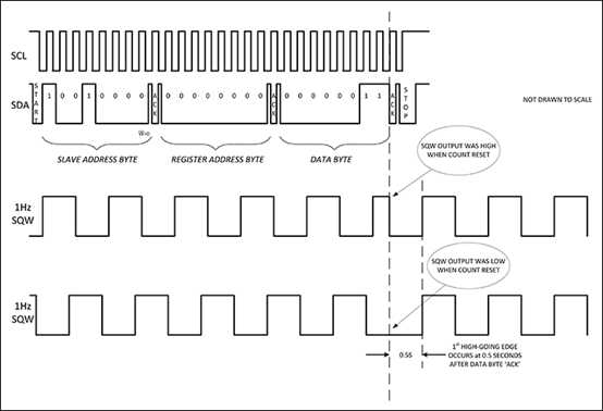
Figure 2. I/O-initiated clock synchronization (I2C format shown).
On the slave‘s acknowledgement of the data byte (27th rising edge of SCL), the slave simultaneously 1) pulls SDA low to ACK receipt of the data byte, 2) the 1Hz countdown chain is reset, and 3) the new Seconds value (03h in the Figure 2 example) is transferred into the Seconds register.
在从机确认数据(SCL的第27个上升沿)时,从机同时1)将SDA拉到ACK接收数据,2)1Hz 倒计时链重置,3)新的秒值(图 2 示例中的 03h)传输到 Seconds寄存器。
On the first 1Hz SQW waveform, the 1Hz signal was Logic 1 when the ACK occurred. SQW is immediately pulled low. Precisely 0.5 seconds after the ACK, the SQW output transitions high. Precisely 1.0 second after the ACK, SQW is pulled low, indicating 1 second has elapsed since the write completed. Reading the Seconds register now results in a content of 04h.
在第一个1Hz SQW波形上,当ACK发生时,1Hz 信号为逻辑 1。SQW立即拉低。在ACK之后0.5秒,SQW输出将转换高电平。在ACK之后精确到1.0秒,SQW被拉低,表示自写入完成以来已过了1秒。现在,读取秒寄存器会得到 04h。
On the second 1Hz SQW diagram, the 1Hz signal was Logic 0 when the ACK occurred, so the SQW signal remains low until precisely 0.5 seconds after the ACK, where the 1Hz output will transition high. Precisely 1.0 second after the ACK, SQW is again pulled low, indicating 1 second has elapsed since the write completed. Reading the Seconds register now results in a content of 04h.
在第二个1Hz SQW图上,当ACK发生时,1Hz信号为逻辑0,因此SQW信号保持低电平,直到ACK之后精确为0.5秒,其中1Hz输出将转换高电平。在ACK之后精确到1.0秒,SQW再次拉低,表示自写入完成以来已过了1秒。现在,读取秒寄存器会得到04h。
For products with 3-wire or SPI I/O, the equivalent trigger to the 27th SCL rising edge in Figure 2 is the next-occurring transition of either SCLK or Chip-Enable (CE or %-overbar_pre%CS%-overbar_post%, whichever input pin naming convention was used).
对于具有3线或SPI I/O的产品,与图2中第27个SCL上升沿相等的触发器是 SCLK 或芯片启用的下一个过渡(CE 或 %-overbar_pre%CS%%-overbar_post%,以使用输入引脚命名约定为准)。
For products with Phantom I/O, the equivalent trigger to the 27th SCL rising edge in Figure 2 is the termination of the 72nd write cycle in the serial data packet (including the 64-cycle pattern recognition).
对于具有幻象I/O的产品,与图2中第27个SCL上升沿相等的触发器是串行数据包中第72个写入周期的终止(包括64周期模式识别)。
For products with Byte-Wide I/O, the equivalent trigger to the 27th SCL rising edge in Figure 2 would be the termination of a write cycle to the Seconds register.
对于具有字节宽 I/O 的产品,与图2中第27个SCL上升沿等效的触发器将是终止到秒寄存器的写入周期。
Using Time-of-Day Alarms
使用日闹钟
On devices with one or more real-time alarm circuits, the user can request either periodic or non-periodic interrupt events to occur at some predetermined time. Alarms can be set up to 30 days in advance of the desired event.
在具有一个或多个实时闹钟电路的设备上,用户可以请求在预定时间发生周期性或非周期性中断事件。闹钟可在所需事件前30天设置。
Programming of the alarms suggests use of a few simple rules:
闹钟的编程建议使用几个简单的规则:
The most common periodic interrupt is a ‘daily alarm‘, set to activate at 5:30AM, fully independent of the calendar content. To ignore the DAY/DATE register, we will utilize an alarm mask.
最常见的定期中断是"每日闹钟",设置为在凌晨 5:30 激活,完全独立于日历内容。要忽略 DAY/DATE 寄存器,我们将使用闹钟掩码。
|
Control = 04h |
oscillator on, define %-overbar_pre%INT%-overbar_post%/SQW output function, alarms off |
|
Alarm1 SECONDS = 00h |
0 seconds |
|
Alarm1 MINUTES = 30h |
30 minutes |
|
Alarm1 HOURS = 45h |
5AM in 12hr Mode |
|
Alarm1 DAY/DATE = 80h |
alarm mask set to match on ‘Hours, Minutes & Seconds‘ |
|
Status = 00h |
clear both alarm flags |
|
Control = 05h |
now enable Alarm1 (A1IE=1) |
At the next occurrence of 5:30AM, the %-overbar_pre%INT%-overbar_post%/SQW pin will assert.
在下次出现5:30AM时,将断言 %-overbar_pre%INT%-overbar_post%/SQW 引脚。
To clear the interrupt, leaving the alarm enabled for the following morning at the same time, clear the associated Alarm Flag (A1F).
要清除中断,在第二天早上同时启用闹钟,清除关联的闹钟标志 (A1F)。
To clear the interrupt and disable any future alarms, clear the associated Alarm Enable (A1IE).
要清除中断并禁用任何将来的闹钟,请清除关联的闹钟启用 (A1IE)。
When the associated alarm is disabled, those alarm registers can be used for general-purpose data storage.
禁用关联的闹钟时,这些闹钟寄存器可用于通用数据存储。
Conclusion
结论
Component initialization procedures, when properly sequenced, should include definitions for all of the RTC‘s hardware functionality required for stable system operation. If desired, the real-time clock can also be synchronized to an external time base, and a procedure for that synchronization has been outlined. Additionally, optional use of real-time clock alarms has been included, focusing upon the order of execution of I/O instructions.
组件初始化过程如果排序正确,应包括稳定系统操作所需的所有RTC硬件功能的定义。如果需要,还可以将实时时钟同步到外部时间基准,并概述了该同步的过程。此外,还可选使用实时时钟闹钟,侧重于I/O指令的执行顺序。
References
引用
Maxim实时时钟芯片设计指南5791-关于编写健壮的实时时钟控制代码的提示
标签:ecif tps seconds time tput ide AMM line which
原文地址:https://www.cnblogs.com/jqdy/p/12307625.html