标签:des style blog http io ar color os sp
Batteries are the typical power sources for portable-system applications, and it is not unusual these days to find microcontroller-based portable systems. A variety of microcontrollers operates at low power-supply voltages, such as 1.8V. Thus you can employ two AA or AAA cells to power the circuit. However, if the circuit requires higher voltage—for LED backlighting for an LCD, for example, which requires approximately 7.5V dc—you must employ a suitable dc/dc converter to boost the power-supply voltage from, for example, 3V to the required voltage. However, you can also employ a microcontroller to develop a suitable dc/dc-boost-voltage converter (Reference 1) with the help of a few additional discrete components.
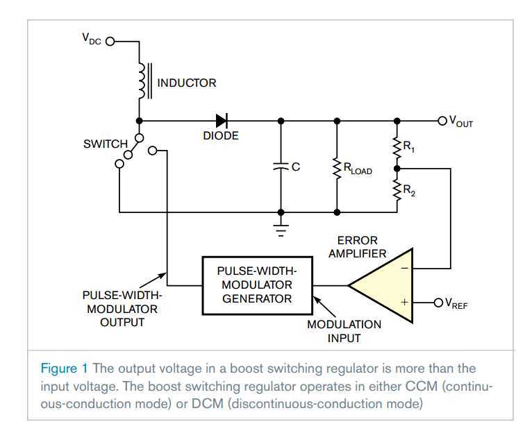
This Design Idea shows how to create not just one, but two dc/dc converters with just a tiny eight-pin microcontroller and a few discrete components. The design is scalable, and you can adapt it for a wide range of output-voltage requirements just by changing the control software for the microcontroller. You can even program the microcontroller to generate any required output-voltage start-up rate. Figure 1 shows the basic topology of a boost switching regulator. The output voltage in such a regulator is more than the input voltage. The boost switching regulator operates in either CCM (continuous-conduction mode) or DCM (discontinuous-conduction mode). It is easier to set up a circuit for DCM operation (Reference 2). The name comes from the fact that the inductor current falls to 0A for some time during each PWM period in DCM; in CCM, the inductor current is never 0A. The maximum current passes through the inductor at the end of high period of the PWM output (when the switch is on) and is:
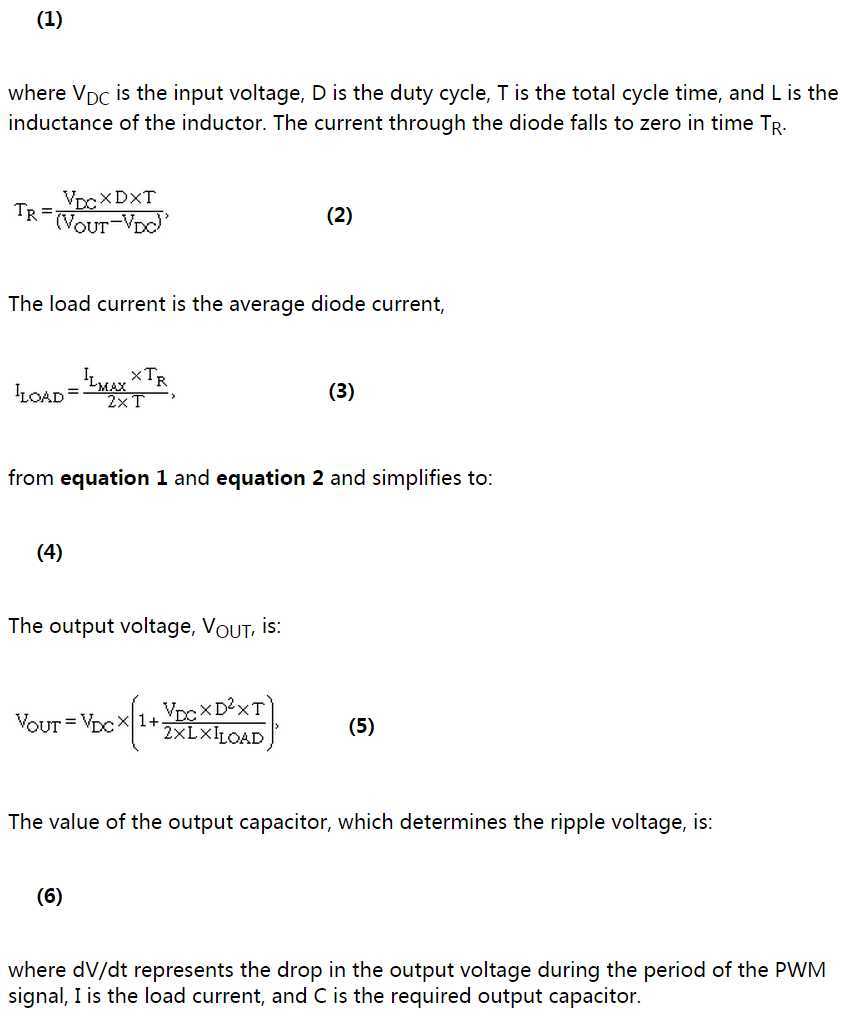
The total period of the PWM wave is T and is a system constant. D is the duty cycle of the PWM wave, and TR is the time during which the diode conducts. At the end of TR, the diode current falls to 0A. The period of the wave is T>D×T+TR for DCM. The difference of the PWM period, T, and (D×T+TR) is the dead time.
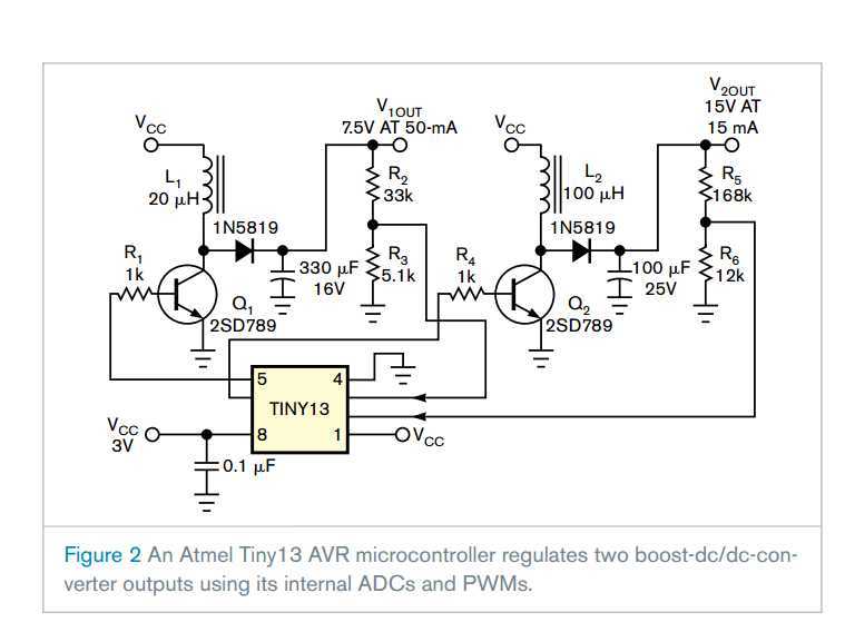
The switch that operates the inductor is usually a BJT (bipolar-junction transistor) or a MOSFET. A MOSFET is preferable because of its ability to handle large current, better efficiency, and higher switching speed. However, at low voltages, a suitable MOSFET with low enough gate-to-source threshold voltage is hard to find and can be expensive. So, this design uses a BJT (Figure 2).
Microcontrollers offer PWM frequencies of 10 kHz to more than 200 kHz. A high PWM frequency is desirable because it leads to a lower inductor value, which translates to a small inductor. The Tiny13 AVR microcontroller from Atmel has a “fast” PWM mode with a frequency of approximately 37.5 kHz and a resolution of 8 bits. A higher PWM resolution offers the ability to more closely track the desired output voltage. The maximum inductor current from Equation 1 is 0.81A for a 20-µH inductor. The transistor that switches the inductor should have a maximum collector current greater than this value. A 2SD789 NPN transistor has a 1A collector-current limit, so it is suitable for this dc/dc converter. The maximum load current achievable with these values, from Equation 4, is 54 mA and thus meets the requirement of maximum required load current for an output voltage of 7.5V.
The Tiny13 microcontroller boasts two high-speed PWM channels and four 10-bit ADC channels. Another PWM channel and an ADC channel create the second dc/dc converter for an output voltage of 15V and a maximum load current of 15 mA. The inductor for this converter has a value of 100 µH. To calculate the output-capacitor value, use Equation 6. For a 5-mV ripple, the value of the capacitor for 7.5V output voltage is 270 µF, because the output current is 50 mA and the PWM-time period is 27 µsec, so this circuit uses the nearest larger value of 330 µF. Similarly, for the 15V output voltage, the required capacitor value is 81 µF, so the design uses a 100-µF capacitor.
The programs for the microcontroller are in C and use the open-source AVR GCC compiler. The AVR Tiny13 microcontroller operates at an internal clock frequency of 9.6 MHz without an internal-clock-frequency divider, so the PWM frequency is 9.6 MHz/256=37.5 kHz. The internal reference voltage is 1.1V. The main program alternately reads two channels of ADCs that monitor the output voltages in an interrupt subroutine. The main program executes an endless loop, monitoring the output voltage by reading the ADC values and adjusting the PWM values accordingly.
  1 #include<avr/interrupt.h>
  2 #include<avr/io.h>
  3
  4
  5 #define vref 931 // 931 is 1V for a 1.1 internal reference
  6 #define MAX_A 70
  7 #define MAX_B 128
  8
  9 volatile unsigned int adc_val[2];
 10
 11 SIGNAL (SIG_ADC)
 12 {
 13 unsigned int temp, temp1;
 14 unsigned char ch;
 15
 16 ADCSRA &= ~(1<<ADEN);//ADC disabled
 17 temp1=ADCL;
 18 temp = ADCH;
 19 temp = temp << 8;
 20 temp =temp | temp1;
 21
 22
 23 ch = ADMUX & 0x01;//channel number
 24 //ch = ch ^0x01;
 25 //ADMUX = ch | 0x40;
 26
 27 if(ch==0)
 28 adc_val[0]=temp;
 29 else adc_val[1]=temp;
 30
 31 ADMUX = ADMUX ^ 0x01; // toggle last bit of MUX to change ADC channel
 32
 33
 34 ADCSRA = 0b11101100; //enable ADC
 35 ADCSRA = 0b11101100;
 36
 37 ch = PORTB ^ 0b00000100;
 38 PORTB = ch;
 39
 40 }
 41
 42 int main(void)
 43 {
 44
 45 unsigned int ad_temp, temp;
 46
 47     DDRB = 0b00000111;
 48
 49
 50     TCCR0A = 0b10100011;
 51 //Fast PWM on OC0A and OC0B
 52 //    TCCR0A - Timer/Counter Control Register A
 53 //    ---------------------------------------------------------
 54 //    |COM0A1|COM0A0|COM0B1|COM0B0|  ?  |  ?  | WGM01| WGM00|
 55 //    |  7   |  6   |  5   |  4   |  3   |  2   |  1   |  0   |
 56 //    ---------------------------------------------------------
 57
 58     TCCR0B = 0b00000001;
 59 //Fed by System Clock of 9 600 000 divided by 1 = 9.6 MHz
 60 //    TCCR0B - Timer/Counter Control Register B
 61 //    -------------------------------------------------
 62 //    |FOC0A|FOC0B|  ? |  ? |WGM02| CS02| CS01| CS00|
 63 //    |  7  |  6  |  5  |  4  |  3  |  2  |  1  |  0  |
 64 //    -------------------------------------------------
 65
 66     ADMUX = 0b01000010; //ADC2 is input to ADC
 67 //    ADMUX - ADC Multiplexer Selection Register
 68 //    -------------------------------------------------
 69 //    |  -  |REFS0|ADLAR|  -  |  -  |  -  | MUX1| MUX0|
 70 //    |  7  |  6  |  5  |  4  |  3  |  2  |  1  |  0  |
 71 //    -------------------------------------------------
 72
 73     ADCSRA = 0b11101100;    //Sampling rate is system clock divided by 16
 74 //    ADCSRA - ADC Control and Status Register A
 75 //    -------------------------------------------------
 76 //    |ADEN |ADSC |ADATE| ADIF| ADIE|ADPS2|ADPS1|ADPS0|
 77 //    |  7  |  6  |  5  |  4  |  3  |  2  |  1  |  0  |
 78 //    -------------------------------------------------
 79
 80     ADCSRB=0;
 81
 82     DIDR0 = 0b00011000;    //Disable Digital input buffer on PB3 and PB4
 83 //    DIDR0 - Digital Input Disable Register 0
 84 //    -------------------------------------------------
 85 //    |  ? |  ? |ADC0D|ADC2D|ADC3D|ADC1D|AIN1D|AIN0D|
 86 //    |  7  |  6  |  5  |  4  |  3  |  2  |  1  |  0  |
 87 //    -------------------------------------------------
 88 adc_val[0]=0;
 89 adc_val[1]=0;
 90 sei();
 91
 92 OCR0A =MAX_A;
 93 OCR0B = MAX_B;
 94
 95 while(1)
 96     {
 97         ad_temp = adc_val[0];
 98
 99         if(ad_temp < vref)
100             {
101
102                     OCR0A++;
103
104                 if( OCR0A > MAX_A)
105                     OCR0A = MAX_A;
106
107             }
108         ad_temp = adc_val[0];
109         if(ad_temp > vref)
110             {
111                     OCR0A--;
112
113                 if( OCR0A > MAX_A)
114                     OCR0A = 0;
115
116             }
117
118         ad_temp = adc_val[1];
119
120         if(ad_temp < vref)
121             {
122
123                     OCR0B++;
124
125                 if( OCR0B > MAX_B)
126                     OCR0B = MAX_B;
127
128             }
129         ad_temp = adc_val[1];
130         if(ad_temp > vref)
131             {
132                     OCR0B--;
133
134                 if( OCR0B > MAX_B)
135                     OCR0B = 0;
136
137             }
138
139     for(temp=0; temp <300; temp++)
140         {    temp = temp +1;
141             temp = temp -1;
142         }
143
144
145     }
146 }
  1 #include<avr/interrupt.h>
  2 #include<avr/io.h>
  3
  4
  5 #define voltref 931 // 931 is 1V for a 1.1 internal reference
  6 #define MAX_A 70
  7 #define MAX_B 128
  8
  9 volatile unsigned int adc_val[2];
 10
 11 SIGNAL (SIG_ADC)
 12 {
 13 unsigned int temp, temp1;
 14 unsigned char ch;
 15
 16 ADCSRA &= ~(1<<ADEN);//ADC disabled
 17 temp1=ADCL;
 18 temp = ADCH;
 19 temp = temp << 8;
 20 temp =temp | temp1;
 21
 22
 23 ch = ADMUX & 0x01;//channel number
 24 //ch = ch ^0x01;
 25 //ADMUX = ch | 0x40;
 26
 27 if(ch==0)
 28 adc_val[0]=temp;
 29 else adc_val[1]=temp;
 30
 31 ADMUX = ADMUX ^ 0x01; // toggle last bit of MUX to change ADC channel
 32
 33
 34 ADCSRA = 0b11101100; //enable ADC
 35 ADCSRA = 0b11101100;
 36
 37 ch = PORTB ^ 0b00000100;
 38 PORTB = ch;
 39
 40 }
 41
 42 int main(void)
 43 {
 44
 45 unsigned int ad_temp, temp, vref;
 46
 47
 48     DDRB = 0b00000111;
 49
 50
 51     TCCR0A = 0b10100011;
 52 //Fast PWM on OC0A and OC0B
 53 //    TCCR0A - Timer/Counter Control Register A
 54 //    ---------------------------------------------------------
 55 //    |COM0A1|COM0A0|COM0B1|COM0B0|  ?  |  ?  | WGM01| WGM00|
 56 //    |  7   |  6   |  5   |  4   |  3   |  2   |  1   |  0   |
 57 //    ---------------------------------------------------------
 58
 59     TCCR0B = 0b00000001;
 60 //Fed by System Clock of 9 600 000 divided by 1 = 9.6 MHz
 61 //    TCCR0B - Timer/Counter Control Register B
 62 //    -------------------------------------------------
 63 //    |FOC0A|FOC0B|  ? |  ? |WGM02| CS02| CS01| CS00|
 64 //    |  7  |  6  |  5  |  4  |  3  |  2  |  1  |  0  |
 65 //    -------------------------------------------------
 66
 67     ADMUX = 0b01000010; //ADC2 is input to ADC
 68 //    ADMUX - ADC Multiplexer Selection Register
 69 //    -------------------------------------------------
 70 //    |  -  |REFS0|ADLAR|  -  |  -  |  -  | MUX1| MUX0|
 71 //    |  7  |  6  |  5  |  4  |  3  |  2  |  1  |  0  |
 72 //    -------------------------------------------------
 73
 74     ADCSRA = 0b11101100;    //Sampling rate is system clock divided by 16
 75 //    ADCSRA - ADC Control and Status Register A
 76 //    -------------------------------------------------
 77 //    |ADEN |ADSC |ADATE| ADIF| ADIE|ADPS2|ADPS1|ADPS0|
 78 //    |  7  |  6  |  5  |  4  |  3  |  2  |  1  |  0  |
 79 //    -------------------------------------------------
 80
 81     ADCSRB=0;
 82
 83     DIDR0 = 0b00011000;    //Disable Digital input buffer on PB3 and PB4
 84 //    DIDR0 - Digital Input Disable Register 0
 85 //    -------------------------------------------------
 86 //    |  ? |  ? |ADC0D|ADC2D|ADC3D|ADC1D|AIN1D|AIN0D|
 87 //    |  7  |  6  |  5  |  4  |  3  |  2  |  1  |  0  |
 88 //    -------------------------------------------------
 89 adc_val[0]=0;
 90 adc_val[1]=0;
 91 sei();
 92
 93 OCR0A = 10;
 94 OCR0B = 20;
 95
 96 vref =190;
 97
 98 while(1)
 99     {
100
101         ad_temp = adc_val[0];
102
103         if(ad_temp < vref)
104             {
105
106                     OCR0A++;
107
108                 if( OCR0A > MAX_A)
109                     OCR0A = MAX_A;
110
111             }
112         ad_temp = adc_val[0];
113         if(ad_temp > vref)
114             {
115                     OCR0A--;
116
117                 if( OCR0A > MAX_A)
118                     OCR0A = 0;
119
120             }
121
122         ad_temp = adc_val[1];
123
124         if(ad_temp < vref)
125             {
126
127                     OCR0B++;
128
129                 if( OCR0B > MAX_B)
130                     OCR0B = MAX_B;
131
132             }
133         ad_temp = adc_val[1];
134         if(ad_temp > vref)
135             {
136                     OCR0B--;
137
138                 if( OCR0B > MAX_B)
139                     OCR0B = 0;
140
141             }
142
143     vref=vref +1;
144     if (vref > voltref)
145         vref = voltref;
146
147     for(temp=0; temp <270; temp++)
148         {    temp = temp +1;
149             temp = temp -1;
150         }
151
152     }
153 }
Tiny microcontroller hosts dual dc/dc-boost converters
标签:des style blog http io ar color os sp
原文地址:http://www.cnblogs.com/shangdawei/p/4127976.html