标签:des blog http io ar os sp for on
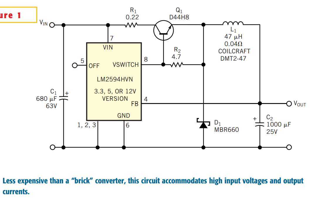
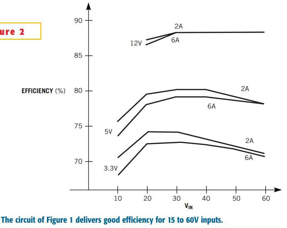
The circuit in Figure 1 uses a minimal number of external parts to raise the maximum output current of a 0.5A buck switching-regulator IC to more than 6A. The circuit accommodates input voltages of 15 to 60V and delivers output voltages of 3.3, 5, or 12V, depending on your choice of IC. Figure 2 provides a graph of conversion efficiency for the three standard output voltages, plotted over a range of input voltages extending to 60V. The circuit is useful in applications requiring higher input voltage, higher current, or both than is available from standard ICs. The LM2594HVN is a buck regulator that switches an internal 0.5A device at 150 kHz. This current suffices to feed the base of Q1 and the bias resistor, R2. The function of R2 is to quickly turn off Q1, a fast npn switch with a beta greater than 10 at 6A. The purpose of R1 may not be obvious without some knowledge of the internal workings of the 2594. Its value is such to produce sufficient voltage drop at peak current so Q1 begins to saturate. The saturation causes Q1‘s beta to drop, and, as the transistor‘s base current rises to more than 0.5A, the 2594 drops into its pulse-by-pulse limited-protection mode, followed by a reduction in clock frequency if the overload is severe.
This design example uses through-hole components, because low-ESR capacitors and inductors in through-hole form are inexpensive and easy to find. Worst-case line and load conditions cause Q1 and D1 to dissipate 3W each, so you must choose a heat-sink size to keep the temperature rise within acceptable limits. A heat-sink rating of 6 to 7°C/W can accommodate both devices for operation to 85°C ambient temperature. The capacitors are low-ESR types from Nichicon‘s PL series (http://www.nichicon-us.com). R2 dissipates less than 0.25W, but, at full load current, R1 can dissipate 1W at high VIN and more than 5W at low VIN. You should locate R1 away from the regulator IC to minimize heating. The DIP version of the 2594 dissipates as much as 0.5W at high VIN; you should solder leads 1, 2, 3, and 6 to a ground-plane area greater than 2 in.2 to avoid thermal shutdown. If you don‘t need the IC‘s on/off feature, then you should also solder Pin 5 to the ground plane.
Bipolar transistor boosts switcher's current by 12 times
标签:des blog http io ar os sp for on
原文地址:http://www.cnblogs.com/shangdawei/p/4128371.html