标签:des style blog code http tar
Embodiments of the invention relate to the field of electronic systems and power management. More particularly, embodiments of the invention relate to a method and apparatus for a zero voltage processor sleep state.
As the trend toward advanced microprocessors, e.g. central processing units (CPUs), with more transistors and higher frequencies continues to grow, computer designers and manufacturers are often faced with corresponding increases in power and energy consumption. Particularly in mobile devices, increased power consumption can lead to overheating, which may negatively affect performance, and can significantly reduce battery life. Because batteries typically have a limited capacity, running the processor of a mobile device more than necessary could drain the capacity more quickly than desired.
Thus, power consumption continues to be an important issue for mobile devices including laptop computers, wireless handsets, personal digital assistants, etc. In today‘s mobile devices, for example, to address power dissipation concerns, certain components may be placed into lower power sleep states based on reduced activity or demand.
For one approach, an operating system may support a built-in power management software interface such as Advanced Configuration and Power Interface (ACPI) (e.g. Advanced Configuration and Power Interface, Ver. x285, June 2004). ACPI describes a power management policy including various "C states" that may be supported by processors and/or chipsets. For this policy, C0?is defined as the Run Time state in which the processor operates at high voltage and high frequency. C1?is defined as the Auto HALT state in which the core clock is stopped internally. C2?is defined as the Stop Clock state in which the core clock is stopped externally. C3?is defined as a Deep Sleep state in which all processor clocks are shut down, and C4?is defined as a Deeper Sleep state in which all processor clocks are stopped and the processor voltage is reduced to a lower data retention point. Various additional deeper sleep power states C5. . . Cn have also been proposed. These additional power states are characterized by equivalent semantics of the C1?through C4?powers states, but with different entry/exit latencies and power savings.
In operation, to enter the deeper sleep states, ACPI may detect a time slot in which there are no new or pending interrupts to the mobile processor. The ACPI policy then uses an input/output (I/O) controller or other chipset features to place the mobile processor into the deeper sleep states.
Once the processor is placed into the deeper sleep state, a break event or interrupt from the operating system or another source may be sent to the chipset, and the chipset will then allow the processor to exit the deeper sleep state. The ability to transition between various power management states, including deeper sleep states, may enable power dissipation to be reduced and battery life to be increased.
Currently, entry into deeper sleep states is done by referencing an external voltage reference in a processor voltage regulator circuit and regulating to this reference voltage whenever a platform "Deeper Sleep" signal such as a DPRSLPVR signal or other similar signal is asserted by the I/O controller or other integrated circuit. The voltage regulator then transitions from a first voltage to a second lower voltage associated with the deeper sleep state. Upon exiting the deeper sleep state, a voltage transition in the other direction takes place with a similar specified time window.
As previously noted, obtaining low power sleep states is important to achieving better battery life in mobile devices. The mobile device market is a fiercely competitive product space and one of the key areas for advancement in this space is low-power solutions to preserve battery life.
Unfortunately, existing deeper sleep states for processors in mobile devices still burn a non-neglible amount of power because voltage is still required to be applied to the processor and cannot be completely powered off.
With reference to FIG. 1, in one embodiment, an integrated circuit device such as a processor, for example, initiates a transition to a zero voltage power management state at block?105. The zero voltage power management state may be, for example, a Deeper Sleep state in accordance with the Advanced Configuration and Power Interface (ACPI) Specification, Revision 2.0a dated Mar. 31, 2002 (and published by Compaq Computer Corporation, Intel Corporation, Microsoft Corporation, Phoenix Technologies Ltd., and Toshiba Corporation). During this transition, the critical state of the processor is saved (block?110). The critical state of the processor includes state variables associated with the architectural, micro-architectural, debug state, and/or similar state variables associated with that processor. The operating voltage of the processor is subsequently reduced to approximately zero such that the processor is in a very deep sleep state that has very low power consumption characteristics (block?115). Hereinafter reference to the state or critical state of the processor or CPU will be meant to include state variables associated with the processor or CPU.
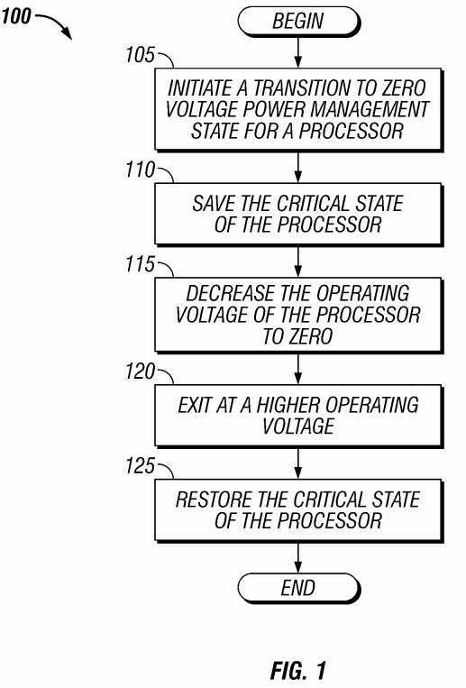
Subsequently, in response to receiving a request to exit the zero voltage power management state, the processor exits the zero voltage power management at a higher reference operating voltage at block?120. The critical state variables associated with the processor are also restored (block?125). It should be noted that for some embodiments, the reference operating voltage may be a minimum active state operating voltage, for example.
FIG. 2 is a block diagram of an exemplary system?200?that may implement the zero voltage power management state transition approach of one or more embodiments. It should be noted that FIG. 2 is divided into?2A and?2B. The system?200?may be a notebook or laptop computer system, or may be any different type of mobile electronic system such as a mobile device, personal digital assistant, wireless telephone/handset or may even be a non-mobile system such as a desktop or enterprise computing system. Other types of electronic systems are also within the scope of various embodiments.
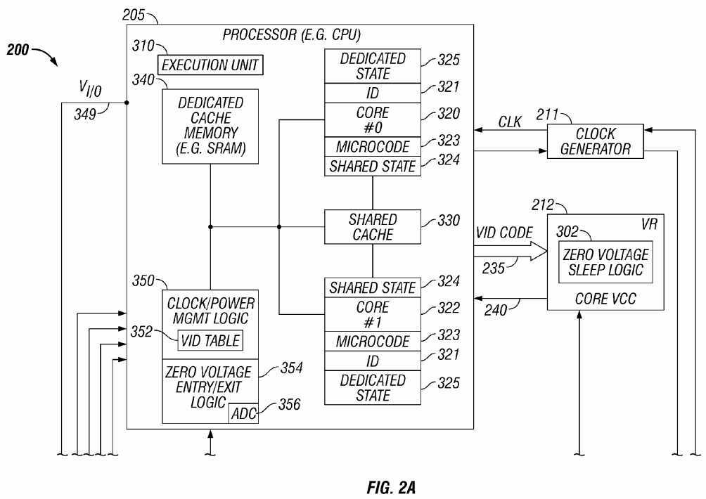
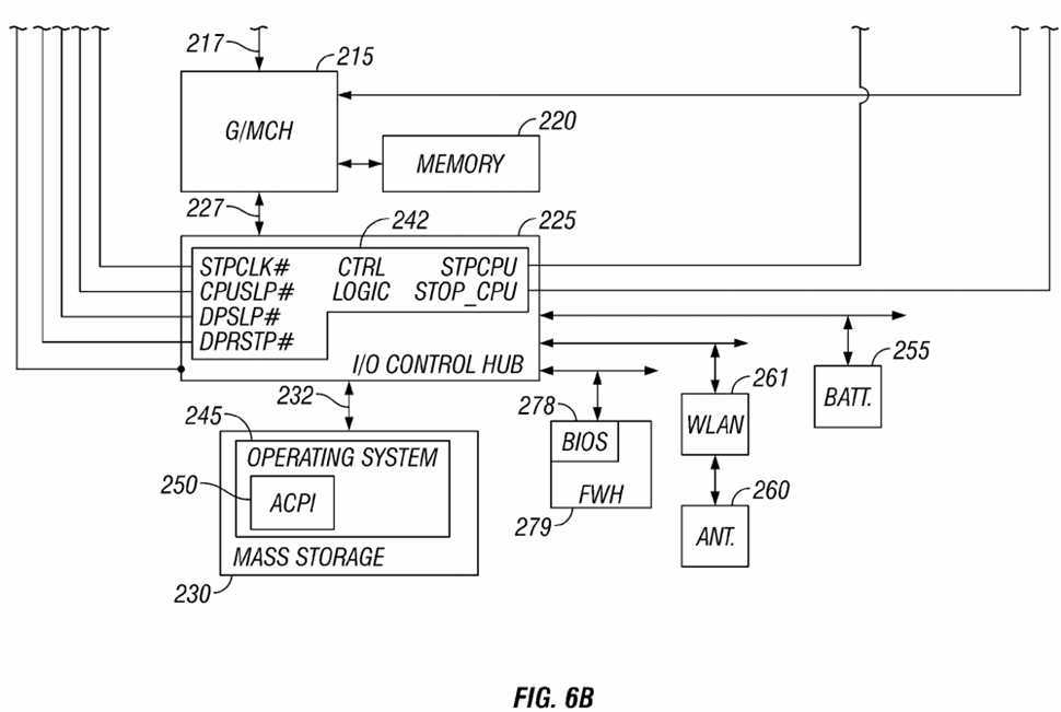
The system?200?includes a processor?205, a platform-level clock generator?211, a voltage regulator?212?coupled to the processor?205, a memory control hub?215?coupled to the processor?205?over a bus?217, a memory?220?which may comprise one or more of random access memory (RAM), flash memory and/or another type of memory, an input/output (I/O) control hub?225?coupled to the memory control hub?215?over a bus?227, and a mass storage device?230?coupled to the I/O control hub?225?over a bus?232. Although, system?200, in one embodiment, may be a mobile device with the subsystems described, it should be appreciated that system?200?may be a different type of mobile device or a non-mobile device, with more or less than the subsystems described.
In one embodiment, the processor?205?may be an Intel? architecture microprocessor such as, for example, a follow-on processor to the Intel Pentium? M processor including one or more processing cores (e.g.?320?and?322) and at least one execution unit?310?to process instructions. For such embodiments, the processor205?may include Intel SpeedStep? technology or another power management-related technology that provides for two or more voltage/frequency operating points. An associated clock/power management unit?350?may be included in the processor?205?to control transitions between two or more of the voltage/frequency pairs.
In other embodiments, the processor?205?may be a different type of processor such as a digital signal processor, an embedded processor, or a microprocessor from a different source.
Further, processor?205?may include a dedicated cache memory?340?(e.g. synchronous random access memory (SRAM)) that may be used to store the processor‘s critical state variables when the processor enters the zero-voltage sleep state, as will be described. Cache memories may be built into the processor‘s chip or packaged within the same housing as the processor chip.
Where Intel SpeedStep? technology or another type of power management technology is included on the processor?205, the available voltage/frequency pairs associated with the technology include a minimum voltage/frequency pair corresponding to a minimum active mode operating voltage and a minimum operating frequency associated with the processor?205?for a fully functional operational mode. These may be referred to herein as the minimum operating voltage and minimum operating frequency or minimum active mode operating voltage and frequency, respectively. Similarly, a maximum operating voltage and frequency may be defined. Other available voltage frequency pairs may be referred to as operating voltage/frequency pairs or simply other voltage/frequency or frequency/voltage pairs.
Zero voltage entry/exit logic?354?may also be included in processor?205, either within or outside of the power management logic?350, to control entry into and exit from the zero voltage sleep state, also referred to herein as the C6?state. The low-power zero voltage processor sleep state will be described in more detail hereinafter.
A voltage identification (VID) memory?352?that is accessible by the zero voltage entry/exit logic?354?may be included to store a voltage identification code look-up table. The VID memory may be an on-chip or off-chip register or another type of memory, and the VID data may be loaded into the memory via software, basic input/output system (BIOS) code?278?(which may be stored on a firmware hub?279?or in another memory), an operating system, other firmware and/or may be hardcoded, for example. Alternatively, a software look-up table including VID and related data may be otherwise accessible by the logic?350. The VID information may also be stored on the CPU as fuses (e.g., programmable ROMs (PROMs)).
An analog-to-digital converter (ADC)?356?may also be provided as part of the zero voltage entry/exit logic?350?to monitor a voltage supply level and provide an associated digital output as described in more detail below.
Voltage regulator?212?provides a supply operating voltage to the processor?205?and may be in accordance with a version of the Intel Mobile Voltage Positioning (IMVP) specification such as the IMVP-6 specification, for example. For such embodiments, the voltage regulator?212?is coupled to receive VID signals from the processor?205?over a bus?235?and, responsive to the VID signals, provides an associated operating voltage to the processor?205?over a signal line?240. The voltage regulator?212?may include zero voltage sleep logic?302?that is responsive to one or more signals to reduce voltage?240?to the processor?205?to a zero state and then ramp the voltage to the processor back up again after exiting the zero voltage sleep state. For other embodiments, a different type of voltage regulator may be used, including a voltage regulator in accordance with a different specification. Further, for some embodiments, the voltage regulator may be integrated with another component of the system?200?including the processor?205. It should be appreciated that the voltage regulator may or may not be integrated with the CPU dependent upon design considerations.
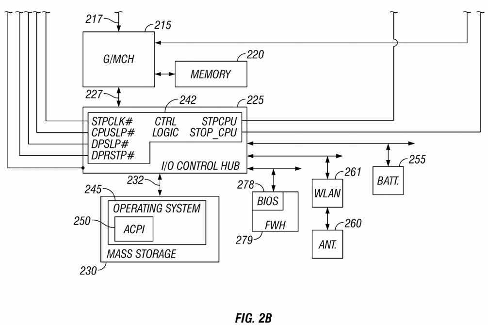
The memory control hub?215?may include both graphics and memory control capabilities and may alternatively be referred to herein as a graphics and memory control hub (G/MCH) or a North bridge. The graphics and memory control hub?215?and the I/O control hub?225?(which also may be referred to as a South bridge) may be collectively referred to as the chipset. For other embodiments, chipset features may be partitioned in a different manner and/or may be implemented using a different number of integrated circuit chips. For example, for some embodiments, graphics and memory control capabilities may be provided using separate integrated circuit devices.
The I/O control hub?225?of one embodiment includes power management state control logic?242, alternatively referred to herein as C-state control logic. The power management state control logic?242?may control aspects of the transitions between some power management and/or normal operational states associated with the processor?205, either autonomously or in response to operating system or other software or hardware events. For example, for Intel? architecture processors for which at least active mode and power management states referred to as C0, C1, C2?and C4?are supported, the power management state control logic242?may at least partially control transitions between at least a subset of these states using one or more of a stop clock (STPCLK#), processor sleep (SLP#), deep sleep (DPSLP#), deeper stop (DPRSTP#), and/or stop processor (STPCPU#) signals as described in more detail below.
Also, in one embodiment, voltage from the I/O control hub?225?(VI/O?349) may be provided to the processor?205?in order to provide sufficient power to the dedicated cache memory?340?such that it can store the critical state variables associated with the processor?205?while the rest of the processor?205?is powered down by the reduction of the operating voltage?240?down to a zero state.
For other types of architectures and/or for processors that support different power management and/or normal operational states, the power management state control logic?242?may control transitions between two or more different power management and/or normal operational states using one or more signals that may be similar to or different from the signals shown in FIG. 2.
The mass storage device?230?may include one or more compact disc read-only memory (CD-ROM) drive(s) and associated disc(s), one or more hard drive(s) and associated disk(s) and/or one or more mass storage devices accessible by the computing system?200?over a network. Other types of mass storage devices such as, for example, optical drives and associated media, are within the scope of various embodiments.
For one embodiment, the mass storage device?230?stores an operating system?245?that includes code?250?to support a current and/or a follow-on version of the Advanced Configuration and Power Interface (ACPI) specification. ACPI may be used to control some aspects of power management as described in more detail below. The operating system?245?may be a Windows? or another type of operating system available from Microsoft Corporation of Redmond, Wash. Alternatively, a different type of operating system such as, for example, a Linux operating system, and/or a different type of operating system-based power management may be used for other embodiments. Further, the power management functions and capabilities described herein as being associated with ACPI may be provided by different software or hardware.
It should be appreciated that, in one embodiment, the processor?205?of FIG. 2 may transition between various known C-states. The normal operational state or active mode for the processor?205?is the C0?state in which the processor actively processes instructions. In the C0?state, the processor?205?is in a high-frequency mode (HFM) in which the voltage/frequency setting may be provided by the maximum voltage/frequency pair.
In order to conserve power and/or reduce thermal load, for example, the processor?205?may be transitioned to a lower power state whenever possible. For example, from the C0?state, in response to firmware, such as microcode, or software, such as the operating system?245, or even ACPI software in some cases, executing a HALT or MWAIT instruction (not shown), the processor?205?may transition to the C1?or Auto-HALT state. In the C1?state, portions of the processor?205?circuitry may be powered down and local clocks may be gated.
The processor may transition into the C2?state, also referred to as the stop grant or SLEEP state, upon assertion of the STPCLK# or similar signal by the I/O controller?225, for example. The I/O controller?225?may assert the STPCLK# signal in response to the operating system?245?determining that a lower power mode may be or should be entered and indicating this via ACPI software?250. In particular, one or more ACPI registers (not shown) may be included in the I/O controller?225?and the ACPI software?250?may write to these registers to control at least some transitions between states. During operation in the C2?state, portions of the processor?205?circuitry may be powered down and internal and external core clocks may be gated. For some embodiments, the processor may transition directly from the C0?state into the C2?state.
Similarly, the processor?205?may transition into the C3?state, also referred to as the Deep Sleep state, in response to the I/O controller?225?or other chipset feature asserting a CPUSLP# signal and then a DPSLP# signal or other similar signals. In the Deep Sleep state, in addition to powering down internal processor circuitry, all phase-lock loops (PLLs) in the processor?205?may be disabled. Further, for some embodiments, a STOP_CPU signal may be asserted by the input/output controller?225?and received by the clock generator?211?to cause the clock generator to halt the clock signal CLK to the CPU?205.
In the system?200?of FIG. 2, a transition into the C4?state or into a zero voltage sleep state may be undertaken in response to ACPI software?250?detecting that there are no pending processor interrupts, for example. ACPI software may do this by causing the ICH?225?to assert one or more power management-related signals such as the exemplary Deeper Stop (DPRSTP#) signal and the exemplary DPSLP# signal. The Deeper Stop (DPRSTP#) signal is provided directly from the chipset to the processor and causes clock/power management logic?350?on the processor to initiate a low frequency mode (LFM). For the low frequency mode, the processor may transition to the minimum or another low operating frequency, for example.
According to some embodiments of the invention, as will be described hereinafter, assertion of the DPRSTP# signal may further cause the internal VID target to be set to a zero voltage level, resulting in a zero operational voltage being applied to the processor?205?by the voltage regulator?212, such that the processor transitions into a very deep sleep state that has very low power consumption characteristics.
According to one embodiment of the invention, an integrated circuit such as processor?205, for example, may initiate a transition to a zero voltage power management state. In one example, processor?205?may be a central processing unit (CPU)?205. Further, the zero voltage management state may be, for example, a deeper sleep state in accordance with ACPI standards. During this transition, the critical state of the CPU?205?may be saved. For example, critical state variables associated with the CPU?205?may be saved in dedicated cache memory (e.g. SRAM)?340.
The operating voltage of the CPU?205?may be subsequently reduced to zero such that the CPU?205?is in a very deep sleep state that has very low power consumption characteristics. Particularly, the voltage regulator?212?utilizing zero voltage sleep state logic?302?may reduce the operating voltage?240?down to zero. As previously discussed, this may be done in conjunction with zero voltage entry/exit logic?354?of clock/power management logic?350?of CPU?205.
In one embodiment, this zero voltage power management state, when implemented in conjunction with ACPI standards, may be referred to as the C6?state.
Subsequently, in response to receiving a request to exit the zero voltage power management state, the CPU?205?exits the zero voltage power management state at a higher reference operating voltage. Particularly, under the control of zero voltage entry/exit logic?354?of CPU?205?and zero voltage sleep logic?302?of voltage regulator?212, as previously described, voltage regulator?212?may raise the reference operating voltage?240?to a suitable level such that the CPU?205?may operate properly. The critical state variables of CPU?205?are then restored from the dedicated cache memory?340.
Thus, the power management scheme allows the CPU?205?to save its state, turn off the power and then wake up when necessary, restore the critical state, and continue where the CPU left off. This may be done, in some embodiments, without explicit support from the operating system?245, and may be accomplished with an extremely short latency period.
More particularly, in one embodiment, in the zero voltage processor sleep state, (which may be referred to as a C6?state in accordance with ACPI standards), the critical state of the CPU?205?is saved in dedicated sleep state SRAM cache?340, which may be powered off the I/O power supply (VI/O)?349, while the core operating voltage?240?for the CPU?205?is taken down to approximately 0 Volts. At this point, the CPU?205?is almost completely powered off and consumes very little power.
Upon an exit event, the CPU?205?indicates to the voltage regulator?212?to ramp the operating voltage?240?back up (e.g. with a VID code?235), relocks the phase lock loop (PLLs) and turns the clocks back on via clock/power management logic?350?and zero voltage entry/exit logic?354. Further, CPU?205?may perform an internal RESET to clear states, and may then restore the state of the CPU?205?from the dedicated sleep state SRAM cache?340, and CPU?205?continues from where it left off in the execution stream. These operations may be done in a very small time period (e.g., approximately 100 microseconds), in CPU?205?hardware, such that it is transparent to the operating system?245?and existing power management software infrastructure.
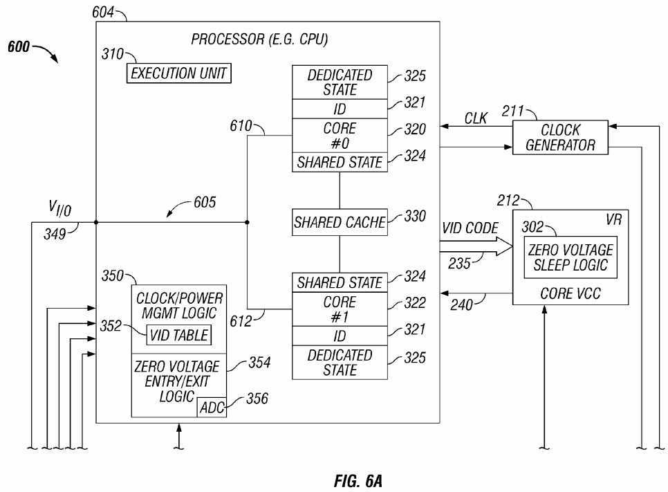
In one embodiment, this methodology is particularly suited for a CPU?205?having multiple processor cores. In this example, core?320?(e.g. Core #0) and core?322?(e.g. Core #1), i.e. a dual-core CPU, will be discussed as an example. However, it should be appreciated that any suitable number of CPU cores may be utilized. In the dual-core structure, the CPU cores?320?and?322?utilize a shared cache?330. For example, this shared cache?330?may be a level 2 (L2) cache?320?that is shared by the cores?320?and?322.
Further, each core?320?and?322?includes a core ID?321, microcode?323, a shared state?324, and a dedicated state?325. The microcode?323?of the cores?320?and?322?is utilized in performing the save/restore functions of the CPU state and for various data flows in the performance of the zero voltage processor sleep state in conjunction with the zero voltage entry/exit logic?354?of the clock/power management logic?350?of CPU?205. Further, dedicated sleep state SRAM cache?340?is utilized to save the states of the cores, as will be described in more detail below.
It will be appreciated that the system?200?and/or other systems of various embodiments may include other components or elements not shown in FIG. 2 and/or not all of the elements shown in FIG. 2 may be present in systems of all embodiments.
Turning briefly to FIG. 3, FIG. 3 is a block diagram illustrating an example of dedicated sleep state SRAM cache?340?and an SRAM interface?364, according to one embodiment of the present invention. The dedicated sleep state SRAM cache?340?may store state variables associated with the architectural, micro-architectural, debug state, and microcode patch when CPU?205?is in the zero voltage sleep state (e.g. the C6?state) previously described.
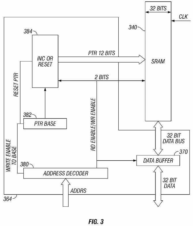
In one example, the size of the SRAM?340?may be 8 KB per CPU core and may be 32 bits wide and may be clocked by the clock/power management logic?350. As previously discussed, the dedicated sleep state SRAM cache?340?may be powered by I/O voltage (VI/O?349) such that its contents are retained when the operating voltage for the CPU?205?is shut off. The dedicated sleep state SRAM?340?may be structured as 2K entries of 32 bits each and may have ECC protection for single bit error detection and correction. The data path may be 32 bits and support a 2-cycle latency into the array. As can be seen in FIG. 3, the SRAM interface?364?may include a 32 bit data bus from a data buffer?370?which utilizes 32 bit data.
In one example, a control register bus interface may be utilized to interface to the microcode in a simple fashion by utilizing a front end cluster interface to reduce the complexity of addressing the SRAM. The interface may use 2K control registers and a two-level addressing scheme. Two registers may be defined to address the SRAM—the first may be a SRAM base register and the second may be an SRAM data register. Microcode may initialize the base register before starting to access the SRAM. The content of the base register may be used as an index into the SRAM for the next read/write to the data register. After every access to the data register, the index into the SRAM may be auto-incremented by one.
As illustrated in FIG. 3, in one example, the SRAM interface?364?may include a data buffer?370?that buffers 32 bit data into and out of SRAM?340?based upon read/write enablement signals from address decoder?380. Address decoder?380?may also enable a write enable to base register?382?and a reset pointer. Base register382?may be used to increment register?384?which operates on SRAM?340?by a 12 bit pointer and a 2 bit read/write enable. Further, based on a reset pointer, register?384?may reset the SRAM.
Turning now to FIG. 4, FIG. 4 is a flow diagram illustrating a process?400?that may be utilized to enter the zero voltage processor sleep state, according to one embodiment of the present invention. In one embodiment, the following series of operations may be directed by the microcode?323?of the CPU cores?320?and?322of CPU?205. In the ACPI embodiment, setting forth the C6?state, the entry into the zero voltage processor sleep state may be initiated via an MWAIT instruction, as previously discussed.
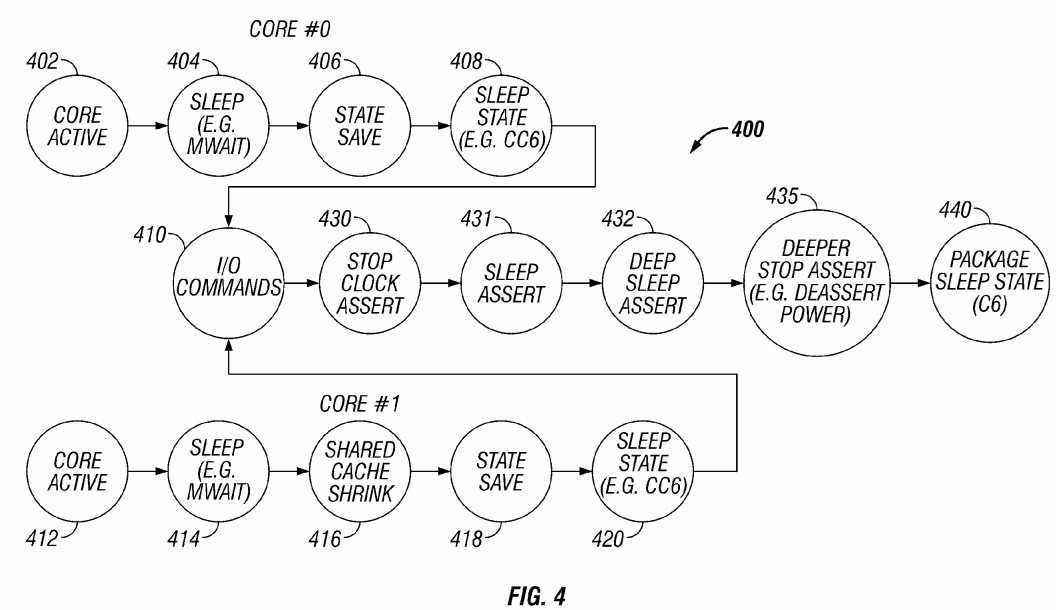
From a software point of view, each CPU core?320?or?322?may independently execute the MWAIT instruction. However, in one embodiment, the CPU cores?320?and?322?utilize an L2 shared cache?330?and the same voltage plane. Hence, in this embodiment, there needs to be hardware coordination in the CPU?205?for package level C states, and particularly, the C6?state.
In this embodiment, each core?320?and?322?may execute an MWAIT instruction, and the initializing CPU core goes into a waiting state (e.g. CC6) and waits for the other core to get into the CC6?state as well, before the whole package (e.g. including both cores?320?and?322) may transition into what may be termed the package C6?sleep state.
Looking particularly at FIG. 4, an illustration of entry into the zero voltage processor sleep state is provided. As shown in FIG. 4, each core independently performs a state save when the zero voltage processor sleep state is initiated. Particularly, looking at CPU core #0?320, the first CPU core #0?is active (circle?402) and then a command for a zero voltage sleep state is initiated (e.g. via a sleep or MWAIT instruction) (circle?404). Responsive to this, the state of CPU core?320?is saved at circle?406?to dedicated cache memory?340. This includes the dedicated state?325?and the shared state?324. CPU core?320?then goes into a first sleep state408?(e.g. CC6) in which it waits for the other core to get into the CC6?state as well, before the whole package can transition into the overall package sleep state (e.g. C6).
In the same manner, the other CPU core (e.g. CPU core #1?322) likewise commands a sleep instruction (e.g. MWAIT) at circle?414?and its state (e.g. both its shared state?324?and dedicated state?325) is also stored to the dedicated cache memory?340?(circle?418). However, in this case, since this is the last core to go into a sleep state, the shared cache?330?is also shrunk and saved to dedicated cache memory?340?(circle?416). Then at circle?420, the second CPU core?322?likewise enters a sleep state (e.g. CC6).
It should be noted that the microcode?323?of the CPU cores?320?and?322?may generally need to know which control registers need to be saved and restored for the zero voltage processor sleep state. The list of the registers may be a subset of the total registers on the CPU?205. For example, the list may be saved as a bit vector (e.g. 1024 bits long). Each bit in the vector may correspond to one control register in the control register address base. For example, microcode may translate the bit position into the control register address and save/restore the register if the bit is "1" and skip it if the bit is a "0". If a control register requires special handling, the save/restore bit in the vector may be set to "0" and the save/restore handled by special microcodes flow outside of the main save/restore loop.
After microcode operations have been performed, as previously discussed, the zero voltage entry/exit logic?354?of the clock/power management logic?350?takes over the data flows (e.g. C6?flows). Particularly, this occurs after the microcode operations are finished as to state saves (406?and?418) and after each CPU core320?and?322?has reached an individual sleep state?408?and?420?(e.g. CC6?state).
At this point, all the required state of the CPU?205?has been saved or flushed from the CPU?205. The zero voltage entry/exit logic?354?of the clock/power management logic?350?then initiates an external platform level entry sequence (e.g. a C6) sequence by performing an I/O register read from the ICH?225. In one embodiment, this may be the ACPI defined method of entering CPU "C" states.
The sequence of events from the external bus perspective from this point is shown in FIG. 4. The I/O commands?410?may be issued from the ICH?225/MCH?215. Particularly, a stop clock signal may be asserted at circle?430?(e.g. STPCLK#). Then, a sleep signal may be asserted. (circle?431) (e.g. SLP#). Further, at circle432, a deep sleep signal may be asserted (DPSLP#). These commands are issued in the previously-described order such that the CPU?205?responds by shutting off its internal clock distribution and then the PLLs.
When at circle?435, a deeper stop signal is asserted (e.g. DPRSTP#), the CPU?205?switches its VID to a zero voltage level in order to tell the voltage regulator?212?to remove power and that it is safe to do so. This may be referred to as a C6?VID. In this way, power is deasserted. However, it should be appreciated that instead of zero volts, an otherwise very small amount of voltage may be chosen as the VID.
It should be appreciated that instead of an exact zero voltage level, the voltage level may set to an "approximately zero voltage level." This approximately zero voltage level may be a very low voltage level, such as 0.3V or 0.5V. In some embodiments, such a very low approximately zero voltage level may optimize entry and exit latencies to and from the sleep state, respectively. Additionally, it should be appreciated, that the approximately zero voltage level may be chosen for the system (e.g. in silicon) during manufacturing (e.g. after a tape-out) and may be programmed differently during different steppings and revisions of the CPU.
The package of CPU cores (e.g. core?320?and core?322) is considered to be in a package sleep state (C6) at circle?440?when the operating voltage?240?from voltage regulator?212?reaches zero volts or another nominally small level. It should be noted that since there is no active device pulling down the operating voltage, it simply drifts down slowly as the charge leaks away due to the CPU?205?leakage. Thus, the CPU?205?has entered the zero voltage package sleep state (C6). It should be appreciated that the sequence of operations previously described may be effectuated in a variety of different orders, and that the previously described order of operations is just one example.
Turning now to FIG. 5, FIG. 5 is a flow diagram illustrating an example of a process?500?for an exit sequence from the zero voltage processor sleep state. Typically, an exit out of the zero voltage processor sleep state begins when the chipset detects an event that necessitates waking up the CPU?205—most likely an interrupt event. However, it should be noted that the chipset may proceed with master accesses to memory without waking up the CPU when doing snoops. The sequence of external events and handshakes that occur between the chipset and the CPU?205?during an exit from the zero voltage processor sleep state will be discussed with reference to FIG. 5. Particularly, this sequence may be considered the reverse of what happens during the previously-described entry phase.
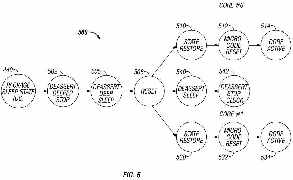
From the package sleep state (C6) (circle?440) in one embodiment, the deeper stop signal (DPRSTP#) is deasserted (circle?502) which is detected by the CPU?205?and the zero voltage entry/exit logic?354?of the clock/power management logic?350?such that the low frequency mode (LFM) VID is sent to the voltage regulator?212. This indicates to the voltage regulator?212?to drive the core operational voltage back up to the required VID.
At a predetermined time (e.g. controlled by timers in the ICH?225), a signal to assert the clocks back on is asserted and the deep sleep (DPSLP#) signal is de-asserted (circle?505), which initiates the PLLs of the clock/power management logic?350. After this, CPU?205?initiates an internal RESET (circle?506). After this reset is complete, CPU?205?has the power and clocks engaged and is ready to restore the critical state variables associated with the CPU?205.
As an example, in the ACPI embodiment, typically during a C-state exit event, CPU?205?waits until the STPCLK# deassertion to do anything internally within the CPU. However, according to embodiments of the present invention, in the zero voltage processor sleep state (e.g. C6) due to the longer latency of restoring the states, etc., STPCLK# is overridden and a state restore (circle?510?and circle?530) for the respective cores?320?and?322?of the CPU?205?is begun in preparation of the C6?exit as soon as the power and clocks are available. Once the states of the cores?320?and?322?are restored, CPU?205?is ready to continue from where it stopped. Microcode?323?from both of the cores?320?and?322?of the CPU?205?are reset (circles?512?and?532), respectively.
However, neither of the CPU cores?320?and?322?become active (circles?514?and?534), respectively, and being executing instructions, until the sleep signal is de-asserted (circle?540) and the stop clock signal (STPCLK#) is de-asserted. However, once the stop clock is de-asserted and the sleep signal is deasserted, both the CPU?205?and cores?320?and?322?and the chipset are all powered on and are operational, and both cores become active (circle?514?and circle?534). CPU?205?then typically begins some code fetches since its caches are empty and then will begin normal operations. More particularly, both cores are woken up in the C0?state. The operating system may determine which CPU core will handle events and the other core may be put back into a sleep state soon thereafter.
Advantageously, as explained earlier, because CPU?205?does the majority of C-state coordination in hardware, software can independently request to enter the zero voltage processor sleep state (e.g. C6) in each core without any software coordination with the other core. More particularly, by utilizing the zero voltage processor sleep state (e.g. C6) the power required by the CPU?205?in the sleep state is reduced virtually to zero.
Also, in the ACPI embodiment, in which the C6?state is described, an efficient method to achieve the state save and the restoration of the shared state?324?of the cores?320?and?322?of processor?205?using a core ID field?321?is also disclosed. This method serves as the synchronization for the core exit into C0. The core identifiers?321?may be hardwired into each core?320?and?322?via fuses and may be available at all times to the cores of the CPU?205.
Both the cores?320?and?322?may save the dedicated state?325?and the shared state?324?at the time of entry. The cores?320?and?322?preferably will not use any ordering method (like a semaphore) during the state save. At the end of the state save, each core may record its unique core identifier?321?in a hardware state.
When the second core completes its state save, that core may write its unique core identifier?321?in the same hardware state, effectively overriding the core identifier of the first core. This hardware state that contains the core identifier will be saved during the C6?residence by powering it with an always ON power source. At C6?exit, as previously discussed, when the cores?320?and?322?perform state restore, the core identifier that matches the stored core identifier will be allowed to perform the restore of the shared state?324. Both cores?320?and?322?may perform the restore of the dedicated state?325. The cores will then access the stored core identifier?321?to check whether they need to perform the restore of the stored state. Merely one core needs to be allowed to perform the restore. The other cores may wait while the shared state?324?is being restored. When the restore is complete, both the cores proceed to the C0?state.
In one embodiment, the cores?320?and?322?may use a hardware semaphore "C6?order semaphore" to ensure exclusive access to the core identifier?321?field during restore. An example of pseudo-code to enable the shared state restore is provided below:
?
In another embodiment of the invention, during the transition to the zero voltage power management state for the processor, the operational voltage applied to the processor by the voltage regulator may be reduced to approximately zero while an external voltage is continuously applied to a portion of the processor that saves the state variables for the processor. For example, the processor may include a voltage plane that applies the external voltage to the portion of the processor to save the state variables that is separate from the operational voltage plane that applies the operational voltage to the processor.
In particular, a system architecture may be provided that allows a processor to enter the zero voltage power management state without utilizing a dedicated cache memory to store the critical state of the processor during the transition to the zero voltage power management state. This may be achieved by utilizing a voltage plane to the processor core that always remains powered. More particularly, an external voltage from an external voltage source (e.g. from the ICH) is continuously applied via the voltage plane to a portion of the processor that saves the state variables of the processor throughout the zero voltage power management state. The portion of the processor that saves the state variables may include model-specific registers (MSRs) and control registers (CRs) of the processor core. In particular, in this scheme, transistors related to model-specific registers (MSRs) and control registers (CRs) of the processor core are placed on the voltage plane which always remains powered.
With reference to FIG. 6, FIG. 6 is a block diagram of an exemplary system?600?that may implement the zero voltage power management state transition approach, previously described, but with a key difference, in that a voltage plane?605?is provided to critical regions of processor cores?320?and?322?of processor?604?that always remains powered to preserve the critical state of the processor cores during the zero voltage power management state. It should be noted that FIG. 6 (shown as FIGS. 6A and 6B) is identical to the previously-described system of FIG. 2 with the exception of a few differences, to be hereinafter described in detail.
In one embodiment, this methodology is particularly suited for a CPU?604?having multiple processor cores. In this example, core?320?(e.g. core #0) and core?322?(e.g. core #1) (i.e. a dual-core CPU), will be discussed as an example. However, it should be appreciated that any suitable number of CPU cores may be utilized. Further, as previously described, in the dual-core structure, the CPU cores?320?and?322?utilize a shared cache?330. For example, this shared cache?330?may be a level 2 (L2) cache?320?that is shared by the cores?320?and?322.
According to one embodiment of the invention, an integrated circuit, such as CPU?604, may initiate a transition to a zero voltage power management state. Further, the zero voltage management state may be, for example, a deeper sleep state in accordance with ACPI standards. During this transition, the critical state of the CPU?604?is continuously kept powered on via voltage plane?605?with power from an external voltage source.
The operating voltage of CPU?604?may be reduced to zero such that CPU?604?is in a very deep sleep state that has very low power consumption characteristics. Particularly, voltage regulator?212?utilizing zero voltage sleep state logic?302?may reduce operating voltage?240?down to zero. As previously described, this may be done in conjunction with zero voltage entry/exit logic?354?of clock/power management logic?350?of the CPU?604. In one embodiment, this zero voltage power management state, when implemented in conjunction with ACPI standards, may be referred to as the C6?state, as previously described.
However, as opposed to the embodiment previously described with reference to FIG. 2, CPU?604?of system?600?does not include a dedicated cache memory (e.g. SRAM?340?as in FIG. 2). This is because voltage plane?605?is provided that continuously provides power to the model-specific registers (MSRs) and control registers (CRs) of the critical portions of processor cores?320?and?322?such that these portions of the processor cores continuously remain powered during the zero voltage power management state (e.g. C6?state). Additionally, because save/restore functions for CPU?604?during the entrance and exit of the zero voltage processor sleep state are not required, microcode sections to enable this functionality are not required (e.g. microcode?322?and?323?of FIG. 2).
Thus, in one embodiment, voltage plane?605?continually provides power to the critical model-specific and control registers for processor cores (#0?and #1)?320?and?322?including registers for the core IDs?321, shared states?324, and dedicated states?325, respectively. In particular, as shown in FIG. 6A, voltage plane?605 includes a voltage line?610?to core?320?and a voltage line?612?to core?322.
However, with respect to the other structural and functional aspects of CPU?604?and the zero voltage power management state previously described with reference to FIG. 2, the structure and functionality is substantially the same, and will not be repeated for brevity‘s sake.
All of the necessary state information for processor cores?320?and?322?needed to resume CPU operations after entry into and exit from the zero voltage power management state is available. This is because the critical portions of processor cores?320?and?322?remain continuously powered during the zero voltage power management state by voltage plane?605.
In one embodiment, voltage plane?605?is continuously powered by the I/O power supply from the I/O control hub?225?shown as VI/O?349. Since CPU?604?includes an always-on voltage plane?605?powering the critical portions of the processor cores?320?and?322, the critical states of the processor cores?320?and?322?of CPU?604?do not have to be saved and restored or "shadowed" to other structures of the CPU (e.g. such as a dedicated cache memory (SRAM)) because, by design, the critical states of processor cores?320?and?322?are never lost because of continuous power being applied by the always-on voltage plane?605. In particular, in one embodiment, the core ID?321, shared state?324, and dedicated state?325?of the processor cores, respectively, are the critical portions that remain powered on by voltage plane?605?during the zero voltage power management state. This voltage plane is maintained irrespective of the operational voltage?240associated with the power plane for entering and exiting the zero voltage power management state (e.g., C6) provided by the voltage regulator?212.
In this embodiment, CPU?604?resumes execution from where it left off before entering the zero voltage management power state by re-powering the zero voltage power management plane (e.g. C6) via operational voltage?240, resetting the transistors in this power plane, and restarting execution based upon the state of the critical state of processor cores?320?and?322?that have continuously remained powered by the always-on voltage plane?605?during the zero voltage management power state. It should be noted that because the number of transistors on the zero voltage power management state (C6) power plane is significantly larger than the number of transistors used to implement the critical-state registers along voltage plane?605?for processor cores?320?and?322?that significant power savings are still achieved.
Thus, according to one embodiment of the invention, CPU?604?may initiate a transition to a zero voltage power management state. During this transition, the critical state of the CPU?604?is continuously kept powered via voltage plane?605. The operating voltage of CPU?604?may be reduced to zero such that CPU?604?is in a very deep sleep state that has very low power consumption characteristics. Particularly, voltage regulator?212?utilizing zero voltage sleep state logic?302?may reduce operating voltage?240?down to zero (e.g., the C6?state). As previously described, this may be done in conjunction with zero voltage entry/exit logic?354?of clock/power management logic?350?of the CPU?604.
Subsequently, in response to receiving a request to exit the zero voltage power management state, CPU?604?exits the zero voltage power management state at a higher reference operating voltage. Particularly, under the control of zero voltage entry/exit logic?354?of CPU?604?and zero voltage sleep logic?302?of voltage regulator?212, as previously described, voltage regulator?212?may raise the reference operating voltage?240?to a suitable level such that CPU?604?may operate properly. The critical state variables of CPU?604?are already present as they have been continually powered throughout the zero voltage power management state by voltage plane?605.
In particular, upon an exit event, CPU?604?indicates to voltage regulator?212?to ramp the operating voltage?240?back up (e.g. with a VID code?235), re-locks the phase lock loops (PLLs), and turns the clock back on via clock/power management logic?350?and zero voltage entry/exit logic?354. CPU?604?then continues from where it left off in the execution stream. These operations may be done in a very small time frame in CPU?604?hardware such that it is transparent to the operating system?245?and existing power management software infrastructure.
Thus, this power management scheme allows CPU?604?to be powered-off and then wake up when necessary and continue where it left off. This may be done, in some embodiments, without explicit support from the operating system?245, and may be accomplished with almost no latency because there is no time needed to save or restore processors states. Moreover, as previously described, the core operating voltage?240?for CPU?604?may be taken down to approximately 0 Volts. At this point, CPU?604?is almost completely powered off and consumes very little power.
As has been described, this methodology is particularly suited for a CPU?604?having multiple processor cores, according to one embodiment. In this example, core?320?(e.g. core #0) and core?322?(e.g. core #1) (i.e. a dual-core CPU), will be discussed as an example. Each core?320?and?322?may include a core ID?321, a shared state?324, and a dedicated state?325?along with other information. However, the core ID?321, shared state?324, and dedicated state?325?are critical sections that remain powered on by voltage plane?605?during the zero voltage power management state. Further, as previously described, in the dual-core structure, the CPU cores?320?and?322?utilize a shared cache?330. For example, this shared cache?330?may be a level 2 (L2) cache?320?that is shared by the cores?320?and?322.
Turning now to FIG. 7, FIG. 7 is a flow diagram of a process?700?for an integrated circuit device, such as a processor (e.g. CPU) to enter and exit voltage power management state. The processor first initiates a transition to a zero voltage power management state (block?705).
During the zero voltage power management state, a separate voltage source is always applied to a portion of the processor to save state variables of the processor (block?710). In particular, a separate external power source is applied in a selective fashion to the processor core to save the critical state of the processor core. As previously described, a voltage plane is provided that continuously provides power to the model-specific registers (MSRs) and control registers (CRs) of the critical portions of processor cores such that these portions of the processor cores continuously remain powered during the zero voltage power management state (e.g. C6?state). These selected critical model-specific and control registers for processor cores (#0?and #1)?320?and?322?may include registers for the core IDs?321, shared states?324, and dedicated states?325, respectively.
Further, as previously described, in the zero voltage power management state, the operating voltage of the processor is reduced to approximately zero (block?715). In this way, the processor is in a very deep sleep state (e.g. C6?state) that has very low power consumption characteristics.
Subsequently, in response to receiving a request to exit the zero voltage power management state, the processor exits the zero voltage power management state at a higher reference operating voltage (block?720).
In this embodiment, because the critical state of the processor core remains powered-on by the always-on voltage plane, the critical state is automatically restored and the processor can continue where it left-off before it entered the zero voltage power management state.
It should be noted that the process for two CPU cores entering the zero voltage management power state utilizing an always-on voltage plane is almost exactly the same as the previously-described process?400?with reference to FIG. 4 and the description applies equally. Therefore, it will not be repeated for brevity‘s sake. The only difference being that process functions?406?and?418?related to the states of the processor cores being saved are not utilized. This is because a dedicated cache memory is not utilized in this embodiment as the critical state of the processor cores are maintained in an always-on state via the voltage plane, as previously described.
Further, it should be noted that the process for two CPU cores exiting the zero voltage management power state utilizing an always-on voltage plane is almost exactly the same as the previously-described process?500?with reference to FIG. 5 and the description applies equally. Therefore, it will not be repeated for brevity‘s sake. The only difference being that operations?510?and?530?are not required because there is no need to restore the state to the processor cores from the dedicated cache. This is because a dedicated cache memory is not utilized in this embodiment as the critical state of the processor cores are maintained in an always-on state via the voltage plane, as previously described. Thus, upon exit from the zero voltage power management state the processor wakes up with the critical state already powered on such that the processor cores can automatically be active. Additionally, there is no need for the microcode reset (operations?512?and?532) to restore the states.
In the previously-described embodiments of FIGS. 4,?5,?6, and?7, it should be noted that save/restore steps?416?and?418?of FIGS. 4 and 510 and?530?of FIG. 5 are not required such that there virtually no latency to enter or exit a low power state because no time is needed to save or restore the processors states.
With reference to FIG. 8, in an alternative embodiment, additional system logic?800?may be provided to a system, such as system?600?of FIG. 6, wherein, instead of merely utilizing a voltage plane?605?to power processor cores additional logic to switch contexts between process cores is also provided.
For example, system logic?800?may include a context logic circuit?802?and a context router?820. In particular, context logic circuit?802?and context router?820?in addition to providing power to processor cores by providing a voltage plane along voltage/signal lines?822?and?824, respectively, also provides for the transfer of digital signal information along voltage/signal lines?822?and?824?such that the contexts of various cores within a CPU, and even between multiple CPUs, may be swapped.
For example, in one embodiment, instead of utilizing voltage plane?605?in CPU?604?of FIG. 6, system logic?800?that includes context logic circuit?802, context router?822, and a first voltage/signal line?822?to processor cores?320?and?322?may be utilized.
Additionally, as particularly shown in FIG. 8, system logic?800?may be utilized to not only enable context switching between multiple processor cores of a single CPU but between multiple processor cores of multiple CPUs. This more generalized multiple CPU system will be discussed hereinafter. However, as will be appreciated by those of skill in this art, this description equally applies to the single CPU case having multiple processor cores as in CPU?604?of FIG. 6.
By utilizing system logic?800, not only do all of the processor cores of multiple CPUs remain powered, but the context of each of the processor cores may be routed to another processor core of the same or a different CPU upon exit of the zero voltage power management state (e.g. C6?state).
As illustrated in FIG. 8, context logic circuit?802?may be powered by voltage (e.g. VI/O?349) from the I/O control hub and may control the routing of different contexts (e.g. context X?810?and context Y?812) in addition to the previously-described provision of the always-on voltage to the critical sections of the CPU cores.
In this example, a first CPU A having multiple cores (0, 1 . . . N)?830,?832?and?834?and a second CPU B having multiple cores (0, 1 . . . N)?840,?842, and?844?is illustrated. Utilizing context router?820, context X?810?and context Y?812, for example, may be routed to any one of the processor cores of the multiple CPUs (CPU A and B) upon exit from the zero voltage management power state via signal lines?822?and?824, respectively. In this way, a very flexible mechanism is provided as to how contexts may be restored to the processor cores of CPUs in a computer system. In particular, based upon core balancing considerations, context logic circuit?802?may restore a context to any suitable processor core within the same CPU or in a different CPU in order to optimize efficiency.
It will be appreciated that, while exemplary embodiments have been described in reference to zero voltage processor sleep state that transitions into and out of a deeper sleep C6?state associated with a central processing unit and voltage regulator, that various embodiments may be applied to different types of power management configurations and/or for different types of integrated circuits. Further, although voltage control is accomplished using VID signals for the exemplary embodiments described herein, other approaches to providing voltage control are within the scope of various embodiments.
SRC=http://www.freepatentsonline.com/8707066.html
PatentTips - Zero voltage processor sleep state,布布扣,bubuko.com
PatentTips - Zero voltage processor sleep state
标签:des style blog code http tar
原文地址:http://www.cnblogs.com/coryxie/p/3789361.html