标签:des style blog code http tar
Many processors include a time stamp count (TSC) counter which is typically implemented as a counter that increments at a fixed rate. Some known TSC counters are clocked at a bus clock rate and a multiplier value is added each bus clock cycle. That is, if the bus clock is at 100 megahertz (MHz) and the processor is stamped for operation at 2000 MHz, a value of 20 is added to the TSC count every bus clock. In general, for a multicore processor there is a single hardware TSC counter for the number of cores present in the processor. The resolved value of the TSC for a given core is this TSC counter value plus a core offset.
Keeping TSC values for each core synchronized in a multi-socket, multi-core and multi-threaded system can be important for software. Certain software uses the TSC value as a stamp to record the order of events, e.g., in a database transaction. Having time going backwards between two processors can cause adverse results, and even can be fatal to some operations. In addition, there can be great complexity involved in enabling a TSC value to be synchronized between multiple cores.
When software is to update the TSC value for a given core, the processor reads the TSC counter and computes a new value. That is, the hardware TSC counter is never written. Because this operation is effectively writing to a moving target, the software is never guaranteed the value it could receive. That is, the various software operations to update the TSC value for a given core can be delayed indefinitely. If the delay occurs in between the software calculation of the new value and writing of this value, the calculation is invalid and the flow will have to be re-performed. Such operations can be common in a single processor system.
Greater complexity is involved in updating TSC values across multiple processors, particularly where these values need to be synchronized for correct software operation. To perform this writing of a TSC value for a core of a multiprocessor system, a more complex flow involving barriers and synchronizations. e.g., pairwise synchronization, is needed, which raises complexity and can be time consuming.
In various embodiments, a time stamp count (TSC) value for a given core (and/or one or more threads executing on the core) can be calculated independently of other cores. Such core TSC values may be based in part on an independent core TSC counter, along with various offsets as will be described below. To this end, reading and writing directly to a core offset can be performed, bypassing the need for synchronization between multiple cores of a multicore processor. As all cores/threads within a socket share a single hardware counter, writing directly to an offset for a core effectively allows software to update a core‘s offset at its leisure. Note this direct writing may be to a thread offset for each of multiple threads executing on one or more cores, as will be described in detail below. In various cases, a core TSC value can be used as a light-weight stamping mechanism to order transactions or to determine the current time of day, for example.
Referring now to FIG. 1, shown is a block diagram of a portion of a processor in accordance with one embodiment of the present invention. As shown in FIG. 1, processor?100?may include uncore logic?110?and core logic?150. In general, uncore logic?110?may include various circuitry, logic, and so forth to perform overall processor operations with regard to power management, interfacing with other components, clocking and so on. In turn, core logic?150?may include the primary execution units of the processor to execute various instructions. In many implementations, processor?100?may be a multicore processor in which a plurality of core logics?150?may be provided, although only a single uncore logic is present.
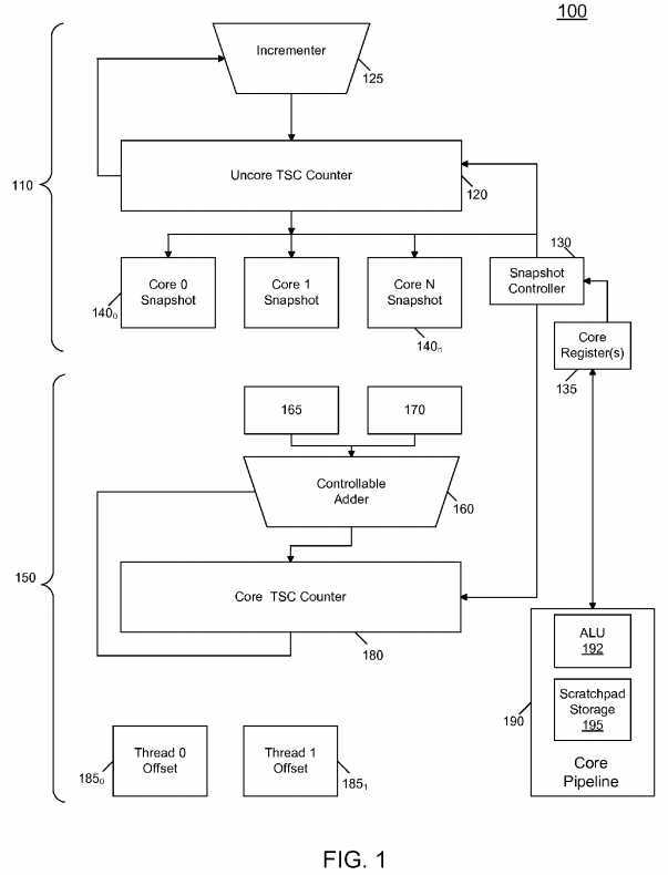
With reference to FIG. 1, primarily shown are components used for purposes of clock operations with regard to time stamp counting, and most other circuitry and logic for the processor is not shown for ease of illustration. With regard to uncore logic?110, an uncore TSC counter?120?may be provided. In general, uncore TSC counter?120?may be incremented by an incrementer?125, e.g., at a rate of a bus clock, namely a bus to which the processor is coupled. In one embodiment, this bus may be a frontside bus (FSB), although the scope of the present invention is not limited in this regard. That is, the term bus is generically used to refer to any type of interconnect, including a serial interconnect such as a point-to-point interconnect. As an example, the processor may be coupled via a point-to-point interconnect and the uncore TSC counter counts according to a common clock rate, which for purposes here may be considered a bus clock rate. The value output by uncore TSC counter?120?may be used for various operations in the uncore. In addition, as will be discussed further below the value from uncore TSC counter?120?may be used by individual cores to permit synchronization between different cores and/or threads executing on the cores.
Still referring to FIG. 1, additional circuitry may be present within uncore logic?110. Specifically, a snapshot controller?130?may be present and may be used to obtain a snapshot for one or more cores. As described below, this snapshot may be a value of the uncore TSC counter at the time of a reset of a corresponding core TSC counter. As seen, a plurality of snapshot storages?1400-140n?may be present, each associated with a given core of the processor. Under control of snapshot controller?130?these snapshot storages may store a current value of uncore TSC counter?120, when enabled by snapshot controller?130. This value stored for a given core may correspond to the time that a TSC counter of the corresponding core logic itself was reset. That is, snapshot controller?130?may generate a reset signal to reset the TSC counter in the core concurrently with the signal to snapshot storages?140?to obtain an uncore TSC counter value. As such, the value stored in a given snapshot storage?140?may correspond to the uncore TSC counter value at reset of a given core TSC counter?180. That is, the uncore TSC counter is a reference and a snapshot is taken at the same time the core TSC counter is reset to zero. These snapshot values may provide a clean point at which to obtain a TSC value from the uncore TSC counter. Then the snapshot value for a given core can be accessed at an indeterminate time and added to the core TSC value, which acts as a reference of time to match the uncore TSC value with the core TSC value.
Regardless of the state of the cores, uncore TSC counter?120?continues to count at its determined ratio and frequency. When different cores enter and exit from different low power states (e.g., so-called C-states of the Advanced Configuration and Power Interface (ACPI) Specification rev. 4 (Jun. 16, 2009)) or other alternate frequency states, the snapshot control mechanism may be used to implement a core frequency update.
In one embodiment, processor microcode may be used to write a register, causing a snapshot to occur and then it reads the snapshot value, polling to ensure the snapshot has been effected. As seen in FIG. 1, in one embodiment this register may be one of a plurality of core registers?135?present in uncore logic?110. This write TSC instruction implemented by processor microcode may thus update a value in a corresponding register for the core in the uncore logic. In turn, this update may trigger snapshot controller?130?to effect an update for the corresponding core snapshot. Thus this control signal to snapshot controller?130?causes the current TSC value of uncore TSC counter?120?to be written into the corresponding core snapshot storage?140. At a (potentially) later time, the value read is written locally into the core. This value may be written from the snapshot storage to a corresponding storage within the core. This snapshot value is thus a static value. As described further below, an effective TSC value for a core is a sum of the core TSC value, a core offset (i.e., this core snapshot value), and a thread offset for a currently running thread.
Still referring to FIG. 1, core logic?150?is next described. In general, core logic?150?may include all the components present to perform instructions, including various storages, ordering logic, execution units, retirement logic and so forth. In the high level view of FIG. 1, such components may generally be shown as a core pipeline?190. In general a core pipeline for an out-of-order machine may include front end units to fetch and decode instructions and an out-of-order engine to reorder the instructions for execution in one or more execution units of the pipeline. The results may then be provided to back end units to reorder and retire the instructions With reference to the timing operations performed, pipeline?190?is shown to include an arithmetic logic unit (ALU)?192. However understand that many more such execution units and logic may be present within core pipeline?190. In addition, one such storage present in a core logic may be a scratchpad storage195, which may be used to provide register-based storage for use by microcode. For example, with reference to the discussion above of the write by processor microcode to core register?135, which triggers a snapshot by a snapshot controller?130, understand that the value written to the corresponding core snapshot storage?140?may be written back to core logic?150, and more specifically may be stored in scratchpad storage?195.
In addition, core logic?150?may include a core TSC counter?180. This counter may be controlled to appear to run at a stamped frequency for the processor. This counter may be updated by a controllable adder?160. In general, core TSC counter?180?may be clocked at a given rate of a core clock frequency. In addition, at predetermined intervals one of a large and/or small adjustment value, stored in adjustment storages?165?and?170?may be added to the count value to thus increment core TSC counter?180?to provide for adjustments when the core is actually executing at a different frequency than the stamped frequency.
That is, a processor is stamped with a particular frequency, e.g., 2 gigahertz (GHz) or 3 GHz, which is the rate at which the core TSC counter is to appear to run. However, because of implementation considerations such as a turbo mode and low power states, the core may be running at a different frequency, e.g., 1 GHz, 4 GHz or other such value. For purposes of various software, the illusion that the core is running at the stamped frequency should be maintained. Because the ratio at which a core may be running versus the ratio corresponding to the stamped frequency may not be multiples of one another, these small and large adjustments can be added to the core TSC value. In one embodiment, the small adjustment can be added every X core clocks, and the large adjustment may be added, e.g., as a least common multiple of when an X core clock lines up with a bus clock. Thus, the core TSC output in general is seen as a stairstep pattern. In one embodiment, the large and small adjustments may be predetermined and programmably calculated, e.g., by processor microcode when a frequency is changed. In one embodiment, this calculation may be in accordance with Equation 1:
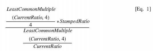
where StampedRatio is the stamped processor frequency and CurrentRatio is the frequency at which a core is operating.
Using Equation 1, the resulting integer quotient is the small adjustment value, and the integer remainder is the large adjustment value. For ease of discussion, these values can be calculated in a slightly simpler fashion in accordance with Equation. 2.?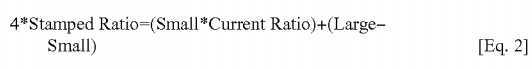
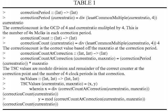
In both equations, 4 is an artifact of the core TSC counter, which adds every fourth clock. This rate merely saves power by avoiding clocking the core TSC counter at a higher rate than it can be read. The correction period is the least common multiple of 4 (since a count occurs every fourth Mclk) and the current ratio divided by the current ratio, which is the greatest common denominator (GCD) of 4 and current ratio multiplied by current ratio. Note the number four is used in this implementation, but other values can be used depending on a resolution at which the TSC counter is read, balanced with the power to be saved by clocking at a lower rate. Table 1 below shows example pseudo code to calculate the large and small adjustments in accordance with an embodiment of the present invention.
Note that the small and large adjustments may be adjusted responsive to the reset signal by snapshot controller?130, in some embodiments.
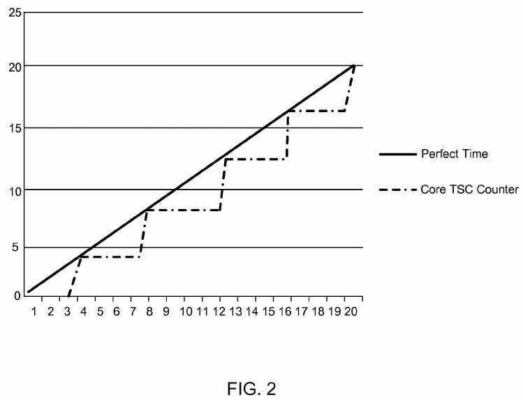
In one embodiment, controllable adder?160?adds the small increment value stored in storage?170?every fourth core clock and adds the large adjustment value stored in storage?165?every fourth core clock that lines up with a bus clock. Referring now to FIG. 2, shown is a comparison of the core TSC counter versus real time. As seen, when a core is running at an odd multiple of the stamped frequency, the small increments are used at all clocks until they match up with a bus clock at which time a large adjustment occurs.
In various embodiments, the two adjustment values stored in storages?165?and?170?can be exposed to software to allow the OS to cause time to speed up marginally without having large discontinuities with time. That is, the OS or other supervisor software can program the small or large adjustment amount, allowing software to tune the core TSC counter to catch up with real time incrementally.
Still referring to FIG. 1, a plurality of thread offset storages?1850?and?1851?may be present in core logic?150, each of which may store a thread offset value. These thread offset values may correspond to an offset for a given thread between the core TSC counter value and the corresponding core offset, obtained from the corresponding core snapshot storage?140. In general, core TSC counter?180?can be used to indicate (by adding the core offset) the length of time from reset that power has been maintained to the core. The thread offset can be software controlled to supply a different perspective of time to the applications running on the core to take account for time spent in a sleep state or to adjust the value for a time of day. Note that while shown with this particular embodiment in FIG. 1, the scope of the present invention is not limited in this regard. For example, synchronization operations as discussed below can be performed in implementations without the core snapshot storages.
In one embodiment, when a read TSC instruction is executed, microcode operates to read the core TSC value and sum the core TSC value, the thread offset and the core snapshot, obtaining an effective TSC value for that thread. In some embodiments a write TSC instruction, which may be a privileged instruction, may cause microcode to sum the core snapshot plus the core TSC counter and calculate what the thread offset would need to be in order to write it to whatever value that the thread wanted, namely a user-defined value. As such, the thread offset value could be a positive or negative number. For example, if the core snapshot was 1000, the core TSC was 2000, and the program instructed a write value of 5000, the thread offset value would become 2000. Note that this write TSC operation acts as a direct write to the thread offset value. In various embodiments, instead of performing a write of the desired core TSC value and then generating a thread offset value whenever software is able to do so, direct access to the thread offset value can occur so that the desired value is directly written to the thread offset value storage. In one embodiment the thread offset value may be stored in a model specific register (MSR). Thus in these embodiments thread offset storages?185?may be implemented as MSRs. Accordingly, a write to this MSR may be performed using a write to MSR instruction. In some embodiments, supervisor software, e.g., an OS, VMM or other privileged software may be used to perform this write to the MSR.
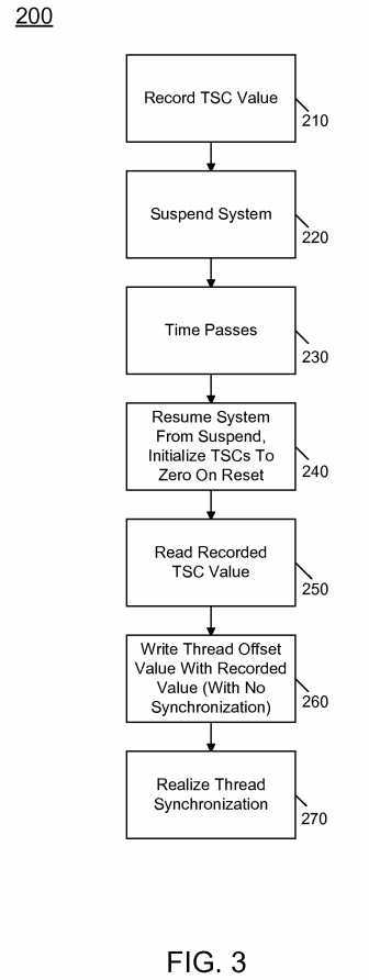
Thus in various embodiments, this thread offset value may be directly written, avoiding the need to perform complex and time consuming synchronization operations between multiple threads. Referring now to FIG. 3, shown is a flow diagram of a method for updating a thread offset value in accordance with one embodiment of the present invention. Note that in various embodiments, the method of FIG. 3 may be performed to enable consistency across threads and cores without a need for any barrier or synchronization operation. Method?200?may be implemented, e.g., using supervisor software such as an OS or VMM, although the scope of the present invention is not limited in this regard. In one particular implementation, a single instruction, e.g., an update TSC instruction, may cause execution of the various operations described in FIG. 3.
As seen, method?200?may begin by recording a TSC value (block?210). In some embodiments, the method of FIG. 3 may be initiated responsive to a user request for a low power state. For example, a user may select a hibernation operation (e.g., via a F4 function key on a laptop keyboard) to cause a system to enter into a standby or hibernate state. Responsive to this selection, the OS or other supervisor software may record a current uncore TSC value to a system memory or to a mass storage (e.g., disk), depending on the given low power state. Then the system may be suspended (block?220). For example, the OS may initiate a so-called S-state to place the system into a suspension state such as an ACPI S3 or S4 state in which various processor entities including both core and uncore logics may be placed in a sleep state in which power to the processor may be completely turned off.
After some amount of time passes (block?230), the system may resume from suspension (block?240). This time may conclude when a user re-initiates operation, or responsive to expiration of a platform timer. At this time, the various time stamp counters, both of the uncore and cores may be initialized to zero on reset. In various embodiments, all TSC counters may be initialized (e.g., all are reset concurrently). Still further in a multi-socket system, all sockets may be reset at the same time.
Because software that was running prior to the suspension had been reading the TSC counter and expecting that value to increase over time, the OS can restore the TSC counter, either to the value before suspension or to a current wall clock time. This decision may be made by the OS, e.g., through a control value. In one embodiment, the wall clock time may be obtained from a real time clock of the system. Thus the recorded TSC value may be read (block?250). Then this recorded TSC value (either the previously stored value or the obtained real time clock value) may be written directly to the thread offset value (block?260). In one embodiment, this thread offset value may be directly written to every thread offset storage for all active threads pending in all active cores at the time of the reset. Note that this write operation may be performed without the need for a synchronization between multiple threads and/or cores.
In this way, a thread synchronization may be realized (block?270) efficiently, without the need for barrier or other synchronization operations. With this recorded thread offset value, a given thread may then execute on a core, using the thread offset value to reflect time as seen by the thread with respect to the core TSC counter (and the uncore TSC counter). Thus at this time, normal counting operations continue with both the uncore TSC counter and the active core TSC counters beginning counting from zero. In one embodiment, at this same time core snapshot storages?140?may also be reset to zero. Thus time as seen by the various threads may be maintained by receipt of the synchronization value and the various calculations discussed above with regard to the core TSC counter value, and the thread offset value (and any updated snapshot values when a frequency is updated for a given core). For other thread offset values or for cores that are not powered up at the same time as the system, the recorded TSC value may be later written when such threads/cores begin execution. Thus, this recorded TSC value acts as a synchronization value that enables updating offsets in different threads/cores to occur at different times but receive the same synchronization value. Still further, this synchronization value can be provided at different times without the need for a synchronization/barrier operation. While shown with this particular implementation in the embodiment of FIG. 3, the scope of the present invention is not limited in this regard.
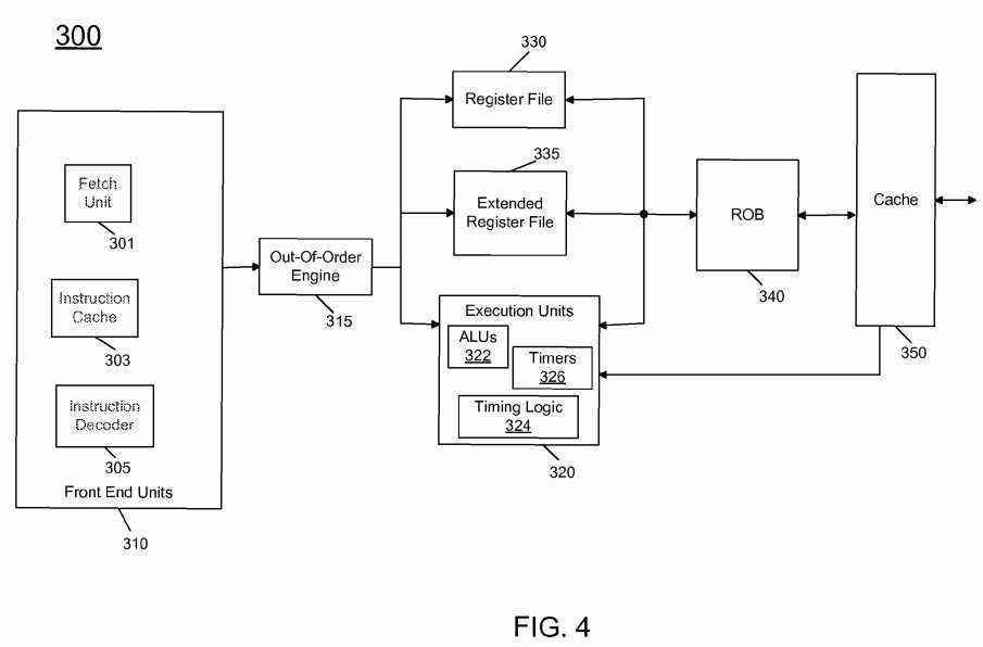
Referring now to FIG. 4, shown is a block diagram of a processor core in accordance with one embodiment of the present invention. As shown in FIG. 4, processor core?300?may be a multi-stage pipelined out-of-order processor. Processor core?300?is shown with a relatively simplified view in FIG. 4 to illustrate various features used in connection with processor wait states in accordance with an embodiment of the present invention.
As shown in FIG. 4, core?300?includes front end units?310, which may be used to fetch instructions to be executed and prepare them for use later in the processor. For example, front end units?310?may include a fetch unit?301, an instruction cache?303, and an instruction decoder?305. In some implementations, front end units?310?may further include a trace cache, along with microcode storage as well as a micro-operation storage. Fetch unit?301?may fetch macro-instructions, e.g., from memory or instruction cache?303, and feed them to instruction decoder?305?to decode them into primitives, i.e., micro-operations for execution by the processor. One such instruction to be handled in front end units?310?may be a TSC update instruction in accordance with an embodiment of the present invention. This instruction may enable the front end units to access various micro-operations to enable execution of the operations such as described above associated with directly updating a thread offset value without the need for a synchronization/barrier operation.
Coupled between front end units?310?and execution units?320?is an out-of-order (OOO) engine?315?that may be used to receive the micro-instructions and prepare them for execution. More specifically OOO engine?315?may include various buffers to re-order micro-instruction flow and allocate various resources needed for execution, as well as to provide renaming of logical registers onto storage locations within various register files such as register file?330?and extended register file?335. Register file?330?may include separate register files for integer and floating point operations. Extended register file?335?may provide storage for vector-sized units, e.g., 256 or 512 bits per register.
Various resources may be present in execution units?320, including, for example, various integer, floating point, and single instruction multiple data (SIMD) logic units, among other specialized hardware. For example, such execution units may include one or more arithmetic logic units (ALUs)?322. In addition, a timing logic?324in accordance with an embodiment of the present invention may be present. Such timing logic may be used to execute certain of the operations involved in performing TSC updates, including controlling one or more ALUs?322?and to perform various operations to directly update a thread offset value. As will be discussed further below, additional logic for handling such updates may be present in another part of a processor, such as an uncore. Also shown in FIG. 4 is a set of timers?326. Relevant timers for analysis here include a core TSC timer and various storages to provide adjustments to the timer value. Results may be provided to retirement logic, namely a reorder buffer (ROB)?340. More specifically, ROB?340?may include various arrays and logic to receive information associated with instructions that are executed. This information is then examined by ROB?340?to determine whether the instructions can be validly retired and result data committed to the architectural state of the processor, or whether one or more exceptions occurred that prevent a proper retirement of the instructions. Of course, ROB?340?may handle other operations associated with retirement.
As shown in FIG. 4, ROB?340?is coupled to a cache?350?which, in one embodiment may be a low level cache (e.g., an L1 cache) although the scope of the present invention is not limited in this regard. Also, execution units?320?can be directly coupled to cache?350. From cache?350, data communication may occur with higher level caches, system memory and so forth. While shown with this high level in the embodiment of FIG. 4, understand the scope of the present invention is not limited in this regard.
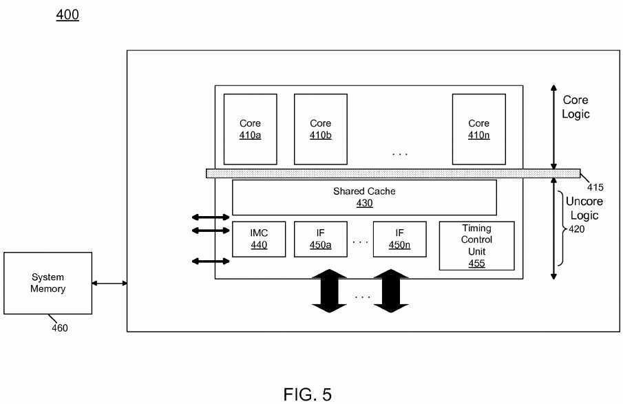
Referring now to FIG. 5, shown is a block diagram of a processor in accordance with an embodiment of the present invention. As shown in FIG. 5, processor?400?may be a multicore processor including a plurality of cores?410a-410n. In one embodiment, each such core may be configured as core?300?described above with regard to FIG. 4. The various cores may be coupled via an interconnect?415?to an uncore?420?that includes various components. As seen, the uncore?420?may include a shared cache?430?which may be a last level cache. In addition, the uncore may include an integrated memory controller?440, various interfaces?450?and a timing control unit?455. At least some of the functionality associated with updating core TSCs may be implemented in timing control unit?455. For example, timing control unit?455?may include the uncore TSC counter, snapshot controller and snapshot storages, such as discussed above in FIG. 1. As seen, processor?400?may communicate with a system memory?460, e.g., via a memory bus. In addition, by interfaces?450, connection can be made to various off-chip components such as peripheral devices, mass storage and so forth. While shown with this particular implementation in the embodiment of FIG. 5, the scope of the present invention is not limited in this regard.
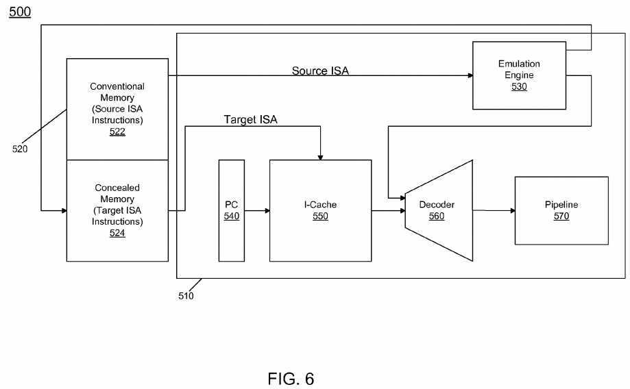
In other embodiments, a processor architecture may include emulation features such that the processor can execute instructions of a first ISA, referred to as a source ISA, where the architecture is according to a second ISA, referred to as a target ISA. In general, software, including both the OS and application programs, is compiled to the source ISA, and hardware implements the target ISA designed specifically for a given hardware implementation with special performance and/or energy efficiency features.
Referring now to FIG. 6, shown is a block diagram of a processor in accordance with another embodiment of the present invention. As seen in FIG. 6, system?500?includes a processor?510?and a memory?520. Memory?520?includes conventional memory?522, which holds both system and application software, and concealed memory?524, which holds software instrumented for the target ISA. As seen, processor?510?includes an emulation engine?530?which converts source code into target code. Emulation may be done with either interpretation or binary translation. Interpretation is often used for code when it is first encountered. Then, as frequently executed code regions (e.g., hotspots) are discovered through dynamic profiling, they are translated to the target ISA and stored in a code cache in concealed memory?524. Optimization is done as part of the translation process and code that is very heavily used may later be optimized even further. The translated blocks of code are held in code cache?524?so they can be repeatedly re-used.
Still referring to FIG. 6, processor?510, which may be one core of a multicore processor, includes a program counter?540?that provides instruction pointer addresses to an instruction cache (I-cache)?550. As seen, I-cache?550?may further receive target ISA instructions directly from concealed memory portion?524?on a miss to a given instruction address. Accordingly, I-cache?550?may store target ISA instructions which can be provided to a decoder?560?which may be a decoder of the target ISA to receive incoming instructions, which may be at the macro-instruction level and to convert the instructions to micro-instructions for execution within a processor pipeline?570. While the scope of the present invention is not limited in this regard, pipeline?570?may be an out-of-order pipeline including various stages to perform and retire instructions. Various execution units, timers, counters, and storages such as described above may be present within pipeline?570?to implement TSC update operations.
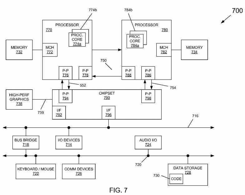
Embodiments may be implemented in many different system types. Referring now to FIG. 7, shown is a block diagram of a system in accordance with an embodiment of the present invention. As shown in FIG. 7, multiprocessor system?700?is a point-to-point interconnect system, and includes a first processor?770?and a second processor?780?coupled via a point-to-point interconnect?750. As shown in FIG. 7, each of processors?770?and?780?may be multicore processors, including first and second processor cores (i.e., processor cores?774a?and?774b?and processor cores?784a?and?784b), although potentially many more cores may be present in the processors. The processor cores may each include core TSC counters that can be updated for given executing threads without the need for a synchronization/barrier operation.
Still referring to FIG. 7, first processor?770?further includes a memory controller hub (MCH)?772?and point-to-point (P-P) interfaces?776?and?778. Similarly, second processor?780?includes a MCH?782?and P-P interfaces?786?and?788. As shown in FIG. 7, MCH‘s?772?and?782?couple the processors to respective memories, namely a memory?732?and a memory?734, which may be portions of main memory (e.g., a dynamic random access memory (DRAM)) locally attached to the respective processors. First processor?770?and second processor?780?may be coupled to a chipset?790?via P-P interconnects?752?and?754, respectively. As shown in FIG. 7, chipset?790?includes P-P interfaces?794?and?798.
Furthermore, chipset?790?includes an interface?792?to couple chipset?790?with a high performance graphics engine?738, by a P-P interconnect?739. In turn, chipset?790?may be coupled to a first bus?716?via an interface?796. As shown in FIG. 7, various input/output (I/O) devices?714?may be coupled to first bus?716, along with a bus bridge?718?which couples first bus?716?to a second bus?720. Various devices may be coupled to second bus?720?including, for example, a keyboard/mouse?722, communication devices?726?and a data storage unit?728?such as a disk drive or other mass storage device which may include code?730, in one embodiment. Further, an audio I/O?724?may be coupled to second bus?720.
? 
SRC=http://www.freepatentsonline.com/8700943.html
PatentTips - Controlling TSC offsets for multiple cores and threads,布布扣,bubuko.com
PatentTips - Controlling TSC offsets for multiple cores and threads
标签:des style blog code http tar
原文地址:http://www.cnblogs.com/coryxie/p/3790224.html