标签:engine 方式 类型 class contain perm cte flash connected
NXP官方提供的手册中 Chapter 8:System Boot中的 Program Image小节中的描述如下:
This section describes the data structures that are required to be included in the user‘s program image. The program image consists of:
(此节描述包含在用户程序镜像中的数据结构,程序镜像由一下部分组成:)
• Image vector table—a list of pointers located at a fixed address that the ROM examines to determine where the other components of the program image are located.
(镜像向量表——位于一个固定地址的指针列表,ROM 检查该地址以确定程序镜像的其他组件的位置)
• Boot data—a table that indicates the program image location, program image size in bytes, and the plugin flag.
(引导数据——一个表指示程序镜像的位置、程序镜像的字节大小和插件标志)
• Device configuration data—IC configuration data.
(设备配置数据- IC 配置数据)
• User code and data.
(用户代码和数据)
The Image Vector Table (IVT) is the data structure that the ROM reads from the boot device supplying the program image containing the required data components to perform a successful boot.
(这个镜像向量表(IVT)是 ROM 从引导设备读取的数据结构,他提供程序镜像,其中包含执行成功引导所需的数据组件)
The IVT includes the program image entry point, a pointer to Device Configuration Data (DCD) and other pointers used by the ROM during the boot process.The ROM locates the IVT at a fixed address that is determined by the boot device connected to the Chip. The IVT offset from the base address and initial load region size for each boot device type is defined in the table below. The location of the IVT is the only fixed requirement by the ROM. The remainder or the image memory map is flexible and is determined by the contents of the IVT.
(这个 IVT 表包含了程序镜像入口点,一个指向设备配置数据(DCD)和 ROM 在引导期间所引用的其他指针。在ROM定位在固定地址的IVT是由连接到芯片的引导设备决定的。每个引导设备的基本地址和初始加载区域大小的IVT偏移量类型在下表中定义。IVT的位置是唯一固定的需求由ROM。余数或图像内存映射是灵活的,由IVT的内容。)
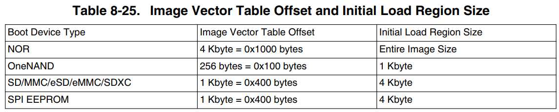
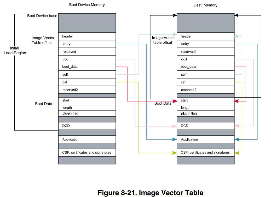
从表中可以看出,引导设备的内存从初始加载区域中的引导设备基址开始执行,然后 IVT 表,Boot Data表
IVT 表的结构
The IVT has the following format where each entry is a 32-bit word:
(IVT 表有以下格式,其中每个条目都是 32 bit)
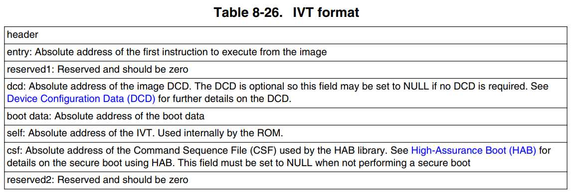
这个表一共列出了 8 个条目,说明 IVT 表的大小就是 4 * 8 = 32 字节

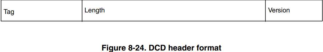
IVT header的格式如上图所示,一个标记,数据长度,版本三个部分组成,构成32位
where:
Tag: A single byte field set to 0xD1
Length: a two byte field in big endian format containing the overall length of the IVT, in bytes, including the header. (the length is fixed and must have a value of 32 bytes)
Version: A single byte field set to 0x40 or 0x41
根据描述可以知道,
Tag:Tag是一个单字节的字段,它的值被设定为0xD1;
Length:一个大端格式的两个字节字段,包含 IVT 的总长度,以字节为单位,包括头。(长度是固定的,值必须为 32 字节)
Version:一个单字节的字段,他的值被设定为 0x40 或者0x41
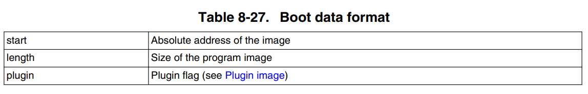
The boot data must follow the format defined in the table found here, each entry is a 32-bit word.
(引导数据必须遵循这里表中定义的格式,每个条目都是一个 32 位 bit)
用之前写的裸机点灯程序用 SD 卡烧录生成的 load.imx使用 winhex打开看看,我们看看他的头部信息是不是与官方提供的手册内容一致
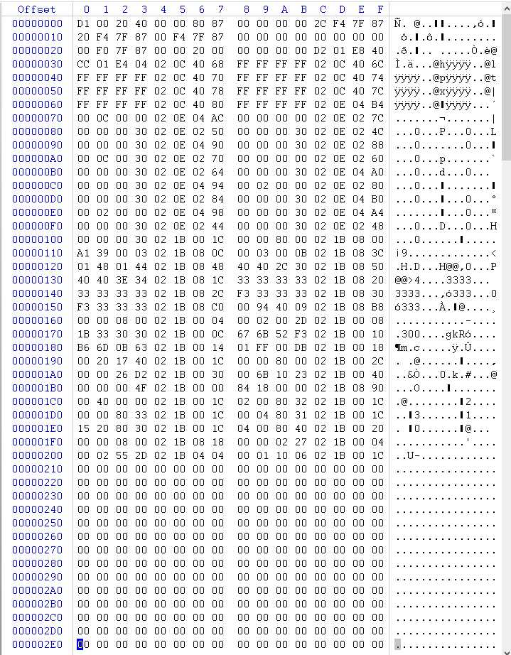
可以看到第一个字节被设为了 0xD1,第二个字节为 0x00,第三个字节为 0x20,第四个字节被设为了0x40,当然也设定为0x41,(0x402000D1),这张图只是截取了 load.imx 的一部分内容,从地址 0x00000000 ~ 0x0000025F,一共 608 个字节的数据
IVT下方紧着就是 Boot Data, IVT 8 个条目,Boot Data 3 个条目,每个条目都是 32 bit,因此 两个加起来共计 44 字节。
将前 44 个字节的数据按照 4 个字节一组组合在一起就是:0x402000D1、0x87800000、0x00000000、0x877FF42C、0x877FF420、0x877FF400、0x00000000、0x00000000、0x877FF000、0x00200000、0x00000000。
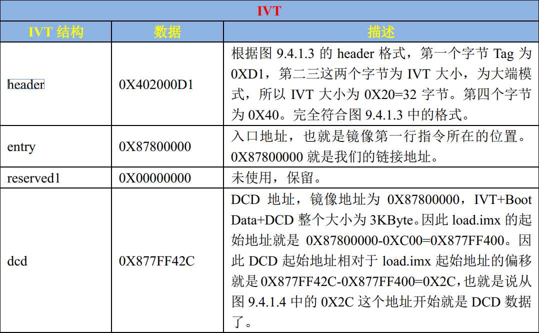
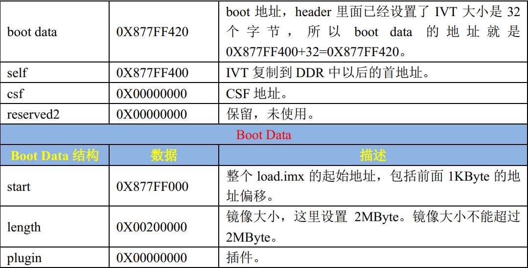
我们详细的列出了 load.imx 的 IVT+Boot Data 每 32 位数据所代表的意义。这些数据都是由 imxdownload 这个软件添加进去的。
Upon reset, the chip uses the default register values for all peripherals in the system. However, these settings typically are not ideal for achieving the optimal system performance and there are even some peripherals that must be configured before they can be used.
(在复位之后,芯片将会为系统中所有的外设使用默认的寄存器值,但是,这些设置通常不是实现最佳系统性能的理想设置,甚至有些外设在使用之前必须进行配置)
The DCD is a configuration information contained in the program image (external to theROM) that the ROM interprets to configure various peripherals on the chip.
(DCD是包含在程序映像(外部到theROM)中的配置信息,ROM解释它来配置芯片上的各种外设。)
For example, the EIM default settings allow the core to interface to a NOR flash device immediately after the reset. This allows the chip to interface with any NOR flash device, but has the disadvantage of slow performance. Additionally, some components (such as DDR) require some sequence of register programming as a part of the configuration before it is ready to be used. The DCD feature can be used to program the EIM registers and the MMDC registers to the optimal settings.
(例如,EIM默认设置允许核心在重置后立即与NOR闪存设备连接。这允许芯片与任何NOR闪存设备接口,但有慢性能的缺点。另外,一些组件(如DDR)在准备使用之前需要一些寄存器编程序列作为配置的一部分。DCD特性可用于将EIM寄存器和MMDC寄存器编程到最佳设置。)
The ROM determines the location of the DCD table based on the information located in the Image Vector Table (IVT). See Image Vector Table and Boot Data for more details. The DCD table shown below is a big-endian byte array of the allowable DCD commands. The maximum size of the DCD is limited to 1768 B.
(ROM根据位于图像向量表(IVT)中的信息确定DCD表的位置。有关更多细节,请参阅图像向量表和引导数据。下面显示的DCD表是允许的DCD命令的大端字节数组。DCD的最大大小被限制为1768 B。)
The DCD header is 4 B with the following format:
where:
Tag: A single-byte field set to 0xD2
Length: a two-byte field in the big-endian format containing the overall length of the DCD (in bytes) including the header
(一个big-endian格式的双字节字段,包含DCD的总长度(以字节为单位),包括头)
Version: A single-byte field set to 0x41
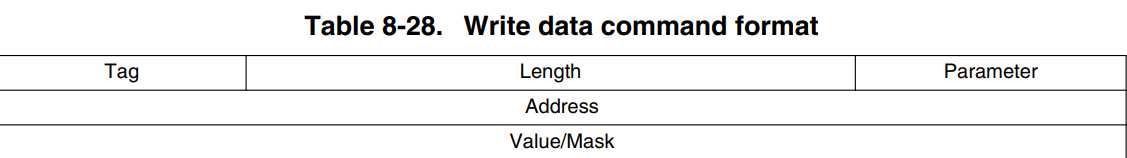
The write data command is used to write a list of given 1-, 2- or 4-byte values (or bitmasks) to a corresponding list of target addresses.
(write data命令用于将给定的1、2或4字节值(或位掩码)列表写入对应的目标地址列表。)
The format of the write data command (in a big-endian byte array) is shown in this table:
(写入数据命令的格式(big-endian字节数组)如下表所示:)
where:
Tag: a single-byte field set to 0xCC
Length: a two-byte field in a big-endian format, containing the length of the Write Data
Command (in bytes) including the header
Address: the target address to which the data must be written
Value/Mask: the data value (or bitmask) to be written to the preceding address
The parameter field is a single byte divided into the bitfields, as follows:
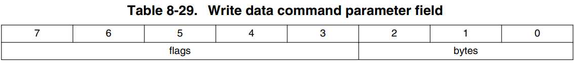
where
bytes: the width of the target locations in bytes (either 1, 2, or 4)---目标位置的宽度(以字节为单位)(1、2或4)
flags: control flags for the command behavior---用于命令行为的控制标志
Data Mask = bit 3: if set, only specific bits may be overwritten at the target address (otherwise all bits may be overwritten)---第3位:如果设置,只有特定的位可能被覆盖在目标地址(否则所有位可能被覆盖)
Data Set = bit 4: if set, the bits at the target address are overwritten with this flag- (otherwise it is ignored) --第4位:如果设置,目标地址的位将被这个标志覆盖(否则将被忽略)
One or more target address and value/bitmask pairs can be specified. The same bytes‘ and flags‘ parameters apply to all locations in the command.
(可以指定一个或多个目标地址和值/位掩码对。相同的字节‘和标志‘参数适用于命令中的所有位置。)
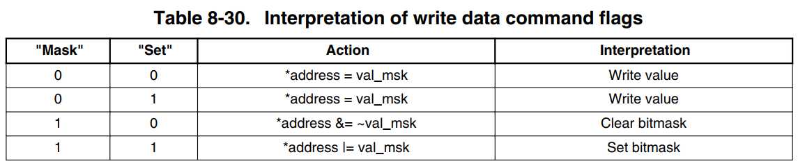
When successful, this command writes to each target address in accordance with the flags as follows:
(当成功时,此命令按照以下标志写入每个目标地址:)
NOTE
If any of the target addresses does not have the same alignment as the data width indicated in the parameter field, none of the values are written.
If any of the values are larger or any of the bitmasks are wider than permitted by the data width indicated in the parameter field, none of the values are written.
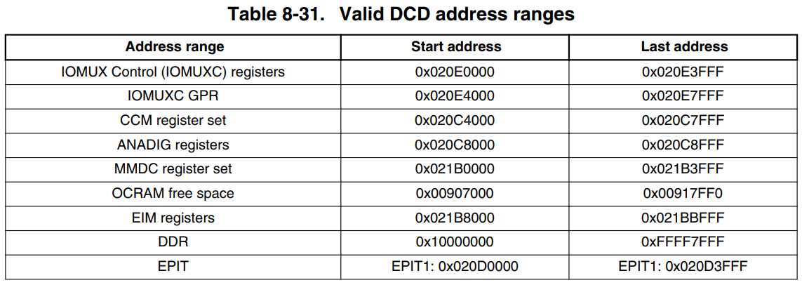
If any of the target addresses do not lie within the allowed region, none of the values are written. The list of allowable blocks and target addresses for the chip are provided below.
( 如果任何目标地址的对齐方式与参数字段中指示的数据宽度不相同,则不写入任何值。
如果任何值大于参数字段中指定的数据宽度所允许的值或任何位掩码的宽度,则不写入任何值。
如果任何目标地址不在允许的区域内,则不写入任何值。下面提供了允许的块和芯片目标地址的列表。)
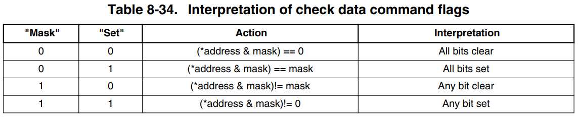
The check data command is used to test for a given 1-, 2-, or 4-byte bitmasks from a source address.
(check data命令用于测试源地址中给定的1字节、2字节或4字节位掩码。)
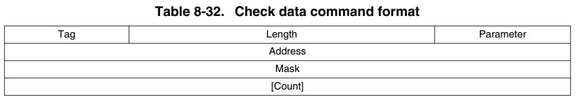
The check data command is a big-endian byte array with the format shown in this table:
(check data命令是一个大端字节数组,格式如下表所示:)
where:
Tag: a single-byte field set to 0xCF——设置为0xCF的单字节字段
Length: a two-byte field in the big-endian format containing the length of the check data command (in bytes) including the header——一个big-endian格式的双字节字段,包含check data命令的长度(以字节为单位),包括头
Address: the source address to test——要测试的源地址
Mask: the bit mask to test——要测试的位掩码
Count: an optional poll count; If the count is not specified, this command pollsindefinitely——计数:可选的投票计数;如果未指定计数,则此命令进行poll确定
until the exit condition is met. If count = 0, this command behaves as for the NOP. ——直到满足退出条件。如果count = 0,则该命令的行为与NOP相同。
The parameter field is a single byte divided into bitfields, as follows:
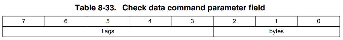
where
bytes: the width of target locations in bytes (either 1, 2, or 4)
flags: control flags for the command behavior
Data Mask = bit 3: if set, only the specific bits may be overwritten at a target address——第3位:如果设置,只有特定的位可能被覆盖在一个目标地址
(otherwise all bits may be overwritten)——否则可能会覆盖所有位
Data Set = bit 4: if set, the bits at the target address are overwritten with this flag——第4位:如果设置,目标地址的位将被这个标志覆盖
(otherwise it is ignored) ——否则它将被忽略
This command polls the source address until either the exit condition is satisfied, or the poll count is reached. The exit condition is determined by the flags as follows:
(此命令轮询源地址,直到满足退出条件或达到轮询计数为止。退出条件由标志决定,如下所示:)
NOTE
If the source address does not have the same alignment as the data width indicated in the parameter field, the value is not read.
If the bitmask is wider than permitted by the data width indicated in the parameter field, the value is not read.
(如果源地址的对齐方式与参数字段中指示的数据宽度不一致,则不读取该值。
如果位掩码的宽度大于参数字段中指定的数据宽度所允许的宽度,则不读取该值。)
This command has no effect. (此命令无效,其实到这就可以不用看了)
The format of the NOP command is a big-endian four-byte array, as shown in this table: (NOP命令的格式为大端四字节数组,如下表所示:)

where:
Tag: a single-byte field set to 0xC0
Length: a two-byte field in big endian containing the length of the NOP command in bytes (fixed to a value of 4)(大端字节的两个字节字段,包含NOP命令的长度(以字节为单位)(固定为值4))
Undefined: this byte is ignored and can be set to any value. (该字节将被忽略,并可以设置为任何值。)
The unlock command is used to prevent specific engine features from being locked when exiting the ROM.(解锁命令是用来防止特定的引擎功能被锁定时退出ROM。)
The format of the unlock command (in a big-endian byte array) is shown in this table: (unlock命令的格式(big-endian字节数组)如下表所示:)
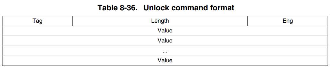
where:
Tag: a single-byte field set to 0xB2(设置为0xB2的单字节字段)
Eng: the engine to be left unlocked (engine 不能上锁)
Values: [optional] the unlock values required by the engine ([可选] engine需要的解锁值)
NOTE: This command may not be used in the DCD structure if the SEC_CONFIG is configured as closed. (如果SEC_CONFIG被配置为closed,那么这个命令可能不会在DCD结构中使用。)
标签:engine 方式 类型 class contain perm cte flash connected
原文地址:https://www.cnblogs.com/Reverse-xiaoyu/p/13388630.html